Review
Manufacturing Graphene and Graphene-based Nanocomposite for Piezoelectric Pressure Sensor Application: A Review
Musaab Khudhur Mohammed 1, Amer Al-Nafiey 2 *, Ghaleb Al-Dahash 2
1 University of Babylon, College of Education for Pure Sciences, Department of Physics, Iraq.
2 University of Babylon, College of science for women, Department of Laser Physics, Iraq.
* Corresponding author. E-mail: pure.musaab.kh@uobabylon.edu.iq
Received: Aug. 29, 2020; Accepted: Dec. 15, 2020; Published: Jan. 11, 2021
Citation: Musaab Khudhur Mohammed, Amer Al-Nafiey, and Ghaleb Al-Dahash, Manufacturing Graphene and Graphene-based Nanocomposite for Piezoelectric Pressure Sensor Application: A Review. Nano Biomed. Eng., 2021, 13(1): 27-35.
DOI: 10.5101/nbe.v13i1.p27-35.
Abstract
Strain sensors have spread at present times, and their electrical resistance has been interpreted. In reality, the use of strain sensors has broadened the reach of technology and allowed us to track changes in the environment in various ways. In recent years, due to their distinctive properties, films based on advanced carbon nanomaterials have started applying sophistication sensing. The strength of the tailored material has been obtained in addition to the various functions applied to these nanomaterials due to the particular structure of the nanomaterials. A prime catalyst for developing nanoscale sensors was this excellent feature. Carbon nanomaterials-based films have been increasing widely due to the excellent properties of nanocomposite-based films for sensing applications (piezoelectric application). There is also an instinctive structure of nanomaterials so that the material is high. Carbon nanomaterials such as graphene are now an excellent alternative for the production of sensors for thermal, electric and mechanical reading.
Keywords: Graphene, Properties, Strain sensor, Piezoelectric
Introduction
In 1856, the scientist Thompson explained the piezeoresitive behavior of iron and copper for the first time and showed that the resisting of these metals changed with the change of elongation. In the other hand geometry played important roles for resistance of materials. The gauge factor is very important to measure sensitivity [piezeoresitive] of sensors also, as a result mechanical strain it is a measures of electrical shift sensitivity. The change in relative resistance to mechanical stress is defined as the change in mechanical resistance and applied strain. The change in this resistance (ΔR) depends on geometric shape and resistivity 𝑅 [3]:
(Δ𝑅/𝑅) = (1 + 2𝑣)𝜀 + Δ 𝜌/𝜌. (1)
This can be proven from the equation, which states that the geometrical distortion effect produces GF (scale factor) from 1.4 to 2, whereas the resistance changes in metals Δ𝜌/𝜌 are smaller (order 0.3) compared to semiconductors such as germanium and silicon where they are 50 to 100 higher of the engineering term [2]. Therefore, researchers seek to identify more advantages of engineering deformation and change of resistance by finding materials with piezeoresitive properties.
The ongoing search for low-cost microprocessors and conventional silicon semiconductors faces challenges and the following research focuses more on nanomaterials [4]. Low-dimensional carbon is very necessary element in the field of nanomaterials [5]. Among the materials that have spread widely because of the very special characteristics of carbon nanotubes and graphene responsible for piezoresistive behaviour, graphene has distinct advantages through its manufacturing method, as it is distinguished from carbon nanotubes, by means of which the manufacturing method is scalable (top-down methods) as well as the ease of obtaining a strain sensor for a transparent layer of graphene compared to other materials. The addition of graphene to the family of nanomaterials is an unusual development in the past decades [6-8]. In the current review, the focus will be on the characterization of graphene-based nanocomposites, their properties, and studies of piezoelectric applications.
Graphene discovery
The graphene structure has been one of the most remarkable discoveries in modern physics over the past 16 years, since 2004 when Andre Geim and his group at the University of Manchester managed to isolate single layers of graphite, namely the graphene. This discovery was a seminal event in the field of optoelectronic materials, and it opened up a wide variety of theoretical and experimental research work in the quantum physics field and in modern physics. Graphene, one of the allotropes of carbon, is a one atom thick sheet of pure carbon, which is the carbon atoms are arranged in a honeycomb structure (hexagons). In 2010, Andre Geim and Konstantin Novoselov were awarded the Nobel Prize for Physics for their "ground-breaking experiments regarding the two-dimensional material graphene". This prize was not just for the discovery of this material, but for their identification of the unique features of graphene that determine its optical and electronic properties [9, 10]. In 1947, P. R. Wallace presented the first report on the unusual semiconducting behavior of graphite and explained the bond structure of graphite by using the new theory of the tight binding model to explain the “superlattice” of bulk graphite [11]. There have been many reports since then describing the electronic properties of graphite, which achieved convergence between theoretical and experimental results, notably McClure (1957), and Slonczewski and Weiss (1958) [12, 13]. After 1958, the experimental work continued to yield data on the two-dimensional graphene layers of this material, and these results were successfully interpreted by a number of researchers such as Boylen and Nozieres (1958) [14], McClure (1958, 1964) [15], Soule et al. (1964) [16], and others. P. R. Schroeder in 1968 provided new results on the location of electrons and holes in graphene by using laser magneto-reflection data [17]. As a result of all these experiments and the characteristics that had been discovered on the structuring of graphene sheets in graphite from 1947, it was scientifically ground-breaking to study and achieve the desired goal of finding an alternative material for the development of many optical and electronic devices. From 1954 to 1972, Linus Pauling succeeded in describing the allotrope of graphite, in his quest into “The Nature of the Chemical Bond”, as consisting of layers of a “giant molecule”, which we know today as graphite [18]. The second type of carbon structure was discovered by Harold W. Kroto and Richard E. Smalley in 1985, namely, fullerene "during experiments aimed at understanding the mechanisms by which long-chain carbon molecules are formed in interstellar space and circumstellar shells" [19]. They were honoured with the Nobel Prize in Chemistry in 1996, and fullerene applications have been playing an important role in all the natural sciences. Actually, in 1970, R. W. Henson was the first scientist to publish a new report on the restructuring of carbon atoms in a football shaped arrangement, but unfortunately, the evidence for this new type of carbon was very weak and was not accepted. In 1991 Sumio Iijima discovered another member of the fullerene structural family of carbon, an allotrope of carbon arranged in a giant cylindrical molecule called the carbon nanotube, when he used an electron microscope to examine carbon [20]. The van-der Waals interactions between atoms of carbon were used to explain many phenomena that occur in graphene planes and in the carbon structures. In 2003 and 2004, Rydberg’s group also reported on their use of the new method of many-body- effects for direct evaluation of both the structure and the binding energy [21, 22].Finally, considering carbon’s role in the chain of life, it is very important to understand the basic structure of graphene and know the electronic and optical properties, as graphene is considered the mother for many types of carbon structures, such as graphite, fullerenes, and carbon nanotubes [23].
Properties of the graphene
Graphene is a 2D planar sheet of sp2-bonded carbon atoms where the atoms are arranged in a honeycomb crystal structure [24]. The carbon–carbon bonds have length of 0.142 nm and 120 degrees angle apart [25]. The bonds between carbon atoms are responsible for their mechanical and thermal properties. The bonds between carbon atoms are responsible for the mechanical and thermal properties. Graphene has the advantage of repairing any holes in its plates in case it is exposed to particles containing carbon. This is a very important feature for many applications. This property works by bombing the pure carbon atom on the graphene sheet, where the carbon atoms apply perfectly to the hexagonal graphene structure and thus fill the holes. It can be wrapped up into 0 dimension fullerenes, rolled into 1 dimension nanotubes or stacked into 3 dimensions as graphite as shown in Fig. 1 [27]. The most significant properties of graphene are summarized in Table 1 [27-31].
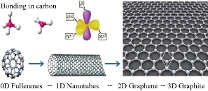
Fig. 1 Graphene in different forms: (a) Wrapped up into 0-dimensional fullerene, (b) rolled into 1-dimensional nanotube, and (c) stacked into 3-dimensional graphite.
Table 1 The physical properties of the graphene
|
Property |
Value |
|
Charge carrier mobility |
~200,000 cm2/V·s |
|
Thermal conductivity |
(3-5)103 W/m·K |
|
Transparency |
~97.4% |
|
Specific surface area |
~2,630 m2/g |
|
Young’s modulus |
~1 TPa |
|
Tensile strength |
~1,100 GPa |
|
Band gap |
0 |
|
Specific density |
2.26 g/cm3 |
|
Resistivity |
2.26 μΩ·cm |
|
Thermal stability |
450-650 ℃ |
|
Melting point |
3,800 K |
|
Current density |
> 108 A/cm2 |
Piezoelectric properties
When we apply mechanical pressure (expansion or pressure), the piezoelectric or piezoelectric materials are generated by electric. Applied pressures produce low voltage due to varying charges resulting from moving electrons and material shape distortion [32]. The intrinsic graphene exits naturally in 2D form and therefore possesses perfect physical symmetry, showing no piezoelectric behaviour. There were, however, many experiments and theoretical predictions that clarify the process of graphene modification or engineering to reach the piezoresponse [33]. Wang et al. [34] measured and studied in plain direct for piezoelectric effect when applying in-plain biaxial strain by using tip of AFM on graphene membranes across the supported-suspended graphene boundary. According to the corresponding work function, the mismatch separates charge and collect them in a region charged by volume. Moreover, the piezoelectric coefficient was experimentally shown as 12.5 μm/V and the direct piezoelectric constants as 37 nC/N [34].
Graphene fabrication is subject to in-depth studies and is an important topic. The research was able to discover the methodology of the researchers from the method of manufacture not only to obtain high-quality graphene but to obtain a surface with a specific surface area [35]. There are very different technique to fabricated graphene, the most widely used methods are chemical peeling, thermochemical synthesis, mechanical bending and chemical vapor deposition [36]. Compound graphene was previously supported on substrates such as minerals and silicon carbide (SiC), but its inability to form two-dimensional structures led to uncertainty of graphene as an independent list until Kostya Novoselvo and Andre Geim made a stunning discovery in which they proposed precise mechanical division (Scotch tape strategy) To break the graphene into a single layer of graphite [37]. In order to better understand the methods mentioned above for graphene synthesis it has been classified as a bottom-up and top-down process. The approaches fall under the top-down strategy category and include mechanical peeling, chemical peel manufacturing, and upward strategies include pyrolysis, overproduction, chemical vapor deposition, and some other methods as well. A top-down method that relies on a raw crushed graphite attack [36].
Mechanical exfoliation
Novoselov and colleagues used this method to discover graphene, and the specific mechanical process employed was scotch tape method [38]. It is formed by Vander Waals forces stacking the graphene stacked onto each other and held in the palace. In comparison to the weak Vander Waals forces between graphene layers, the in-line carbon bonds are stronger. The energy and distance to the interlayer bond is 2 eV / nm2 and 3.34, respectively, and mechanically allow external forces about 300 nN/μm2 to cleave graphite to monolayer graphene [39]. Graphite flake is sandwiched between scotch tapes for mechanical exfoliation through scotch technique and then graphite flakes are repeatedly cleaved through scotch tape. Finally, scotch tape with connected graphene is scrub onto SiO2/Si substrates (or other desired substrates) to remove graphene layer [40]. This is repeated until a mono or a little layers of graphene are gained.
Chemical exfoliation
This method needs exfoliating the graphite in an arrangement. It could be a flexible strategy for creating graphene suspension, and is in a perfect world suited to best down approaches among others. Graphene is ordinarily hydrophobic, but oxygen connection that incorporates useful bunches such as epoxide, hydroxyl, carbonyl and carboxy changes graphene to hydrophilic surfaces. The oxidized graphite can be scattered in water, and graphene oxide monolayer can be picked up by centrifugation and ultra-sonic in water or other fitting dissolvable [40]. The choice of dissolvable is imperative because it can offer assistance to make strides the dissolvability of graphene [41]. Hernandez et al. [41] showed that the dissolvable surface pressure between 25 and 69 mJ/m2 was perfect for chemical exfoliation [41]. The moment organize incorporate ultra-sonic or fast warming to segregate or exfoliate graphene into mono or graphene in a small layers [39].
Chemical reduction of graphite oxide
There is a method for producing graphene in large quantities, which is the method of reduction, and reducing graphite oxide is a top-down method to obtain it. The graphite industry is often oxidized graphite oxide. Graphite is oxidized through the use of (oxidizers such as concentrated sulfuric acid and nitric acid) [39]. However, single layer graphite oxide films are reduced by other methods such as thermal or chemical methods. Hydrazine is considered to be the chemically reduced graphene oxide (CRGO), while thermal reduction occurs by annealing in the hydrogen / argon environment called thermogenic graphene oxide (TRGO) [42]. The graphene acquired from both processes possesses little quality compared to the method of adhesive tape [43]. Comparatively, the chemical reduction of graphite oxide dispersion in water requires the use of ultrasound exfoliation, accompanied by the scattering of graphene oxide dispersed by the introduction of hydrazine [44].
Epitaxial growth
The strategy comes under the bottom-up category. This is one of the methods on the surfaces by which graphene is synthesized. In addition, these were surfaces to generate graphene less than 10 nm in thickness. This method include Silicon carbide crystals being heated and cooled. Through this process, crystals of SiC decomposed by annealing with high temperature as a first step. Heating desorbs silicone from the surface and produces surface layer of carbon because of carbon atom accumulation. Pressure, temperature and rate of heating are very important for this process as they are monolayer, bilayer, trilayer and specific temperatures at constant pressure can generate more layer graphene [40].
Chemical vapor deposition
It is a favorable process for collecting graphene on a large scale. In this process, graphene is created on catalytic substrates such as copper and nickel by the chemical decomposition of substances (precursors), such as methane, methanol, ethanol and acetylene [45]. Nickel is the most widely used catalytic transition-metal substrate. CVD requires four stages, precursors with a carbon content diffuse in the first step and are absorbed on the substrate surface. In the second stage molecules are released on precursor pyrolysis and carbon ad-atoms surface substratum. The next step is to dissolve carbon ad-atoms on the substratum surface. The temperature is then decrease to saturate the solution, and carbon atoms precipitate out of solution as a consequence of forming graphene films [46]. At the edges / boundaries of the grain nickel shapes grains of multilayer graphene. In addition, due to considerable carbon solubility in nickel, graphene on the nickel surface during precipitation poses a problem of multilayer growth [47].
Pyrolysis
The thermal method for solvo is the common method recorded for manufactured graphene by pyrolysis in literature. The ethanol and sodium were thermally reacted in a closed container at a ratio of 1:1. Graphene sheets were smoothly separated by pyrolizing of graphene ethoxide with the aid of ultra-sonic tubes. Graphene sheets were manufactured to a maximum of 10 μm. The advantages of this method include high purity graphene with simple manufacturing system, low temperature graphene functionalization and low production cost. Yet the graphene generated is of low quality due to defects on the graphene surface
Graphene/polymer nanocomposite
Polymer nanocomposites based on carbon black, carbon nanotubes, and layered silicates used for different application such as thermal, mechanical, electrical, and gas barrier properties [48-50]. A new class of polymeric nanocomposites was created when graphene was discovered, as it has unique physical properties and excellent propagation through the polymer matrix. Polymer / graphene compounds have also demonstrated improved mechanical and thermal properties, obstructions and flame retardants. [51-54]. Hence, graphene is seen, from its inception, as a versatile filter for the manufacture of polymeric nanocomposites. The improvement in the properties of the resulting compounds depends on the extent of interconnection between the filler and matrix. One of the important functions of graphene is that it increases the binding to the polymeric matrix in addition to the high compatibility between them. This feature is unique and important for the many applications [55].
Synthesis of graphene/polymer nanocomposite
Graphene/polymer compounds can be prepared with a different technique like site polymerization, mixing solution and melting blend.
Site polymerization
One of the effective techniques for uniformly dispersing graphene and its derivatives in a polymer matrix is the situ polymerization technique [56]. In this technique, initially graphene or auxiliary heat or radiation [56, 57]. Thereafter, the polymer is assumed to be inoculated on the surface of graphene or its derivatives resulting in fine dispersion and good adhesion between the derivative component in the monomer followed by polymerization with a wide range of polymer compounds such (LDH - polystyrene sulfonate (PSS)), (LDH - Polyimide (PI)), as (graphene – PMMS), (graphene – PS) and (graphene – PMMA) compounds [58-64].
Mixing solution
In the method of mixing the solution, graphene is dispersed first in a solvent (aqueous and organic) and then mixed with the auxiliary polymer by ultra-sonic with mechanical stirring followed by evaporation of the solvent. A wide range of polymer compounds such as graphene / PVA, EVA / LDH, graphene / PMMA, graphene / PU, etc. are treated with solution mixing technology [65-68]. In soluble mixing technology, it is highly efficient when the polymers don't enter the solution or aren't suitable for polymerization at the site.
Melting blending
Melting blending technology has been found to be particularly suitable for the manufacture of thermoplastic composites. This process has an important principle, as the first polymers are heated to form a viscous solubility, after which high shear forces are applied to disperse graphene particles through the polymer, after which the casting process is used. Polypropylene, polylactide, polyethylene terephthalate, etc. were widely used to manufacture the compound after melted mixing [69, 70].
Piezoelectric strain sensors
Recently, the interest in flexible sensors has increased greatly due to its great compatibility with arbitrary and satisfying curved surfaces and its widespread use in many fields including (wearable electronics, healthcare, communications and environment, electronics and robots, etc.) [71]. The focus of flexible stress sensors has been on structural health monitoring and human health monitoring. Traditional metal and ceramic stress sensors suffer from inherent brittleness and hardness, fabricated from complex manufacturing processes and cannot meet the needs and requirements of rapidly growing engineering application [72]. Strain sensors for composite of nanomaterials have important characteristics such as low cost and lightweight; high flexibility. They can be manufactured easily and sensitively. In addition, it was also improved by optimizing the technique of synthesis and infiltration using a suitable nano filler [73]. The rapid progress in the nanotechnology fields has helped to develop sensitive materials for stress sensors in the past decade. To demonstrate the required piezoelectric properties, number of materials like graphene, black carbon particles, metallic nanostructures and polymeric nanofibers have been manufactured [74, 75].
Application of graphene based for the piezoelectric pressure Sensors
The piezoelectric pressure sensor is very important device for engineering and industrial applications. These sensors help monitor pressure as it affects the sensor surface. Electrochemical properties made the nanomaterials applicable to pressure sensing applications. Table 2 shows a comparison between the important features of the different graphene based nanoscale sensors.
Table 2 Piezoelectric pressure sensor
|
Materials |
Fabrication Technique |
Sensitivity (kPa-1) |
Pressure Range (kPa) |
Remark |
Reference |
|
rGO / P(VDF-TrFe) |
Electrospinning technology |
15.6 |
-- |
1. The piezoelectric sensor demonstrated a high level of stability over 100,000 cycles, with a response time of 5ms at the expense of a low voltage of about 1 V. 2. The low 1.2 Pa limit of detection can detect rice grain and even a feather. 3. The higher limit of detection and high integration of the area further increase the application further sensor can be used to monitor torsion and bending, blood pressure and distribution of spatial pressure. |
[76] |
|
rGO / Tisse paper |
Soaking / Thermal reduction |
17.2 |
0 to 20 |
1. The tests performed under different pressures, namely 400, 600, 2500 and 20000 Pa, demonstrate a good stable response, while the change in relative resistance is important due to a slight change in pressure. 2. In terms of sensitivity, the multilayer performed better but showed greater hysteresis, mainly due to air gaps between graphene paper, and the two types of sensors were compared, namely single and multilayer. 3. The sensor displayed different responses to each word when applied to the throat of the tester speaking words "hello" "sensor" and "graphene," indicating a high degree of sensitivity. Method / Drop casting / Laser scribing technology for GO / DVD disk hummers from 0.96 0 to 50 1. demonstrated by the sensor. |
[77] |
|
Graphene / Copper / PMMA |
CVD / Spin coating |
110 |
75 |
1. With a low detection limit of 0.2 Pa and a rapid response of less than 30 ms, and excellent repeatability and stability for 10,000, the sensor showed excellent performance. Cycles for loading / unloading. 2. By putting two 3D grown graphene films face to face on PDMS into a flexible sensing framework, the sensor was manufactured. 3. The sensor showed that subtle human movements such as phonation and wrist movements and sounds were successfully detected by pf. |
[78] |
|
Graphene / PDMS |
Sandwich |
7.68 |
-- |
1. The sensor was 3.19 kPa-1 sensitive with an ultra-low detection limit of 1 mg and a fast response of 30 ms. 2. It is evident from the experiment that MGrE electrodes will increase the sensitivity of the sensor as both top and bottom electrodes. More sensitivity can be regulated by the controllable micro conformal structure. 3. The study of finite elements shows that compressibility of the microstructure and contact area decide piezoresistive response. |
[79] |
|
Graphene / PDMS |
Direct laser scribing |
480 |
-- |
1. The sensor demonstrated a relaxation time / fast response of (3μs/2μs) with excellent stability for pressure below 28 Pa over 4000 loading / unloading cycles. 2. The sensor has a 5 V operating voltage with a low 160 μW power consumption. 3. The sensor revealed the ability for spatial pressure distribution and epidermal electronics to be observed. |
[80] |
|
WGF / PVA |
Hummers method / Poured and dried |
28.34 |
-- |
1. The sensor has a porous bubble structure with an uneven surface and serves as a filler material for PVA. 2. Under a pressure application, "point to face", "face to face" and point to point "work well and provide short paths of transmission." 3. Even for a rice grain of 22.4 mg, the device showed good sensitivity and showed good repeatability for 6000 cycles. |
[81] |
|
GPN / PDMS-nickel |
CVD / Thermal heating / Soaking |
0.09 |
1000 |
1. The sensor demonstrated good motion detection at loading and unloading pressure and stretching cycles at 1666 kPa pressure and 25 percent strain. 2. The sensor displayed a rapid response with falling and rising times of 80 and 100 ms respectively to external loading. |
[82] |
|
Graphene / PDMS |
Self-assembled |
1875.53 |
0 to 40 |
1. In a detection range of 1 to 40 kPa, the sensor demonstrated a good trade-off between linearity and sensitivity. 2. The sensor had a high peak signal noise ratio of 78 dB with good stability, resulting in a universal wearable sensor and a high precision wearable sensor being constructed. 3. The sensor showed good stability for 15,000 loading and unloading cycles under three loads of 8.5,15 and 40 kPa with a low detection limit of 1.8 Pa and a rapid response of 2 ms. |
[83] |
|
GFET |
CVD / Spin coating |
4.55×10⁻³ |
0 - 94.18 |
1. Using a low temperature CMOS compatible method in combination with transfer printing, the piezo-potential controlled extended gate GFET pressure sensor has been developed. 2. The sensor works at a very low voltage of 100 mV, allowing for future use in applications such as wearable electronics and electronic skin applications. 3. During the cyclic switching test, the sensor displayed a stable response over 400 cycles with no visible deterioration in its efficiency, showing its usability for real-world applications. |
[84] |
|
rGO / Polyurethane / Selenium |
Hummers method / Freeze drying |
0.22 |
0.09 to 30 |
1. Depending on the construction material, the sensitivity of the sensors is divided into different parts, such as rGO foam, rGO / PU foam and SFrGO / PU foam, with a sensitivity of 15.22, 0.22 and 46.67 kPa-1 for a pressure range of 0 to 0.3, 0.09 to 30 and 48 to 72 kPa-1 respectively. 2. The sensor functions as a multi-meter switchable pressure sensor with high 1000-fold repeatability along with an ultra-high improvement in resistance. |
[85] |
Conclusions
For nanotechnology applications, the discovery of graphene has altered several ideas. For mechanical, electrical, optical and electromechanical applications, this material has proven to be excellent. In a round dimensional structure (0D) called fullerene, graphene is encapsulated and wrapped in a curved cylindrical structure (1D) called carbon nanotubes, and graphite is formed when stacked on each other. The thinnest nanometer is graphene and is the most potent substance ever tested. The technologies used for the collection of graphene have recently been commercially developed, and most of the methods used are chemical vapor deposition. Due to their significance in sensor applications, the study addressed graphene-based nanomaterials, in particular polymer-based materials. Therefore, in this work, an important graphene as the piezoelectric pressure sensor and the commercial application of graphene were documented in detail.
Acknowledgments
Praise be to Allah Lord of the World, and best prayers and peace upon him best messenger Mohammed, his pure descendants, and his noble companions. Then, I would like to express my deep gratitude and appreciation to my supervisors, Dr. Ghaleb Al-Dahash, Dr. Amer Al-Nafiey for their guidance, suggestions, and encouragement throughout the research work.
Conflict of Interests
The authors declare that no competing interest exists.
References
Copyright© Musaab Khudhur Mohammed, Amer Al-Nafiey, and Ghaleb Al-Dahash. This is an open-access article distributed under the terms of the Creative Commons Attribution License, which permits unrestricted use, distribution, and reproduction in any medium, provided the original author and source are credited.

|
Nano Biomedicine and Engineering. Copyright © Shanghai Jiao Tong University Press |
 |