Review
Ordered Arraysof Carbon Nanotubes: From Synthesis to Applications
Huiyang Liu, Guangxia Shen*
Department of Bio-Nano Science and Engineering, Key Laboratory for Thin Film and Micro fabrication Technology of Ministry of Education, National Key Laboratory of Micro /Nano Fabrication Technology, Research Institute of Micro/Nano Science and Technology, Shanghai Jiao Tong University, Shanghai, 200240, P.R. China.
* Corresponding author. Emial: gxshen@sjtu.edu.cn
Citation: H.Y. Liu et al. Ordered Arrays of Carbon Nanotubes:From Synthesis to Applications Nano Biomed. Eng. 2012, 4(3), 107-117.
DOI: 10.5101/nbe.v4i3.p107-117.
Abstract
Carbon nanotubes are well known for their unique physical properties, which depend on the dimensions of the nanotubes. It is imperative to develop methods for positioning, orienting, and controlling the diameter and length of CNTs before they can be used in a broad range of applications. This review will focus on the synthesis of ordered CNTs. A few promising applications that are expected to impact emerging technologies are also introduced.
Keywords: Carbon Nanotubes Array, Template Nanolithography, Contact Printing, Dip-pen biosensor
1. Introduction
Carbon nanotubes (CNT) synthesis has evolved from enabling growth into consciously controlling the growth driven by many aspects of basic research and practical applications requirements. Most of the application will require the carbon nanotubes (CNTs) with uniform, well-defined and controllable properties. For example, in electronic and photonic devices, emission displays and data storage would need high density, well-ordered nanotube arrays. [1,2] As usual, arc-discharge,[3] laser ablation,[4] and chemical vapor deposition[5] have been the three main methods used for carbon nanotubes (CNT) synthesis. The first two employ solid-state carbon as precursors to fabricate CNTs and involve carbon vaporization at high temperatures. Chemical vapor deposition (CVD) utilizes hydrocarbon gases as sources and metal catalyst particles as “seeds” for CNT growth that take place at relatively lower temperatures. While arc-discharge and laser ablation methods produce only tangled CNTs mixed randomly with byproducts, the CVD grows nanotube arrays at controllable locations with desired orientations on catalytic patterned substrate surfaces. So CVD method combined with different strategy to direct the orientation of CNTs has become the most promising way to realize the growth of ordered CNTs with high qualities. At its earlier period, people mainly focused on how to grow high-quality arrays of carbon nanotubes. When synthesis is no longer the key point, structure control at the macroscopic level mainly its orientation, and at the microscopic level, such as length and diameter, took place. However, the precise placement of CNTs, this very specific 1D nanomaterial, as blocks, in the right place with right configuration and with exceedingly high densities, are still a daunting. In this review, we will focus on the several synthesizes of ordered CNTs. main applications of well-ordered CNTs arrays will be also introduced including transistor and photovoltaic, filed emission, biosensing etc. The intrinsic properties of CNTs that being utilized are, for example, their semi- conductivity, Electrical and Optic properties etc.[6]
2. Preparation Methods of CNT Arrays
Thermal Evaporation technique, which mostly done by a tube furnace, is the most popular method. This not only due to the low cost of equipment, but also due to the ease of apparatus setup and the freedom of manipulating materials growth. It is used to grow structures, like nanotubes, nanowires, and nanoparticles aided by several different types of chambers and growth- enhancing methods. The presence of a catalyst, either
predeposited on the substrate or provided in the gas feedstock, activates the chemical reaction between the substrate surface and the gaseous precursor.[7] In order to fabricate well-ordered CNTs arrays, several strategies have been employed, such as assembling CNTs selectively on catalytically patterned substrate, template- assisted growth of CNTs arrays using porous substrate, or post-assembly CNTs from their suspension.[8, 9] But the post-assembly would be caused the destruction of their intrinsic properties due to the harsh treatment of CNTs in. [10, 11] In the following, the other two strategies will be introduced and discussed.
2.1 Template-assisted growth of CNTs arrays using porous substrate
Thermal Evaporation technique works with Template assisted synthesis, such as the use of Anodized Aluminum Membrane (AAM),[12] is a promising tool for the controlled growth of CNTs arrays. J. Li, C. Papadopoulous, and J. M. Xu have fabricated large arrays of parallel carbon nanotubes with good periodicity and uniformity by pyrolysis of acetylene on cobalt within a hexagonal close-packed nanochannel alumina (NCA) template. [13] A typical fabrication process flow is shown in Fig. 1. The process begins with the anodization of high purity (99.999%) aluminum on a desired substrate. The next step is to electrochemically deposit a small amount of cobalt catalyst into the bottom of the template channels. The CO flow is then replaced by a mixture of acetylene in nitrogen. In template-assisted method, the growth of CNT arrays is subject to the restrictions of the pore, and can only be in the axial direction of the pore elongation. In this process, due to the restrictive effect of the pore, the curvature become relatively smaller, which indicates that the pores can limit the growth of CNTs, and can make the grew CNTs more straight, leading to less arrays and surface defects. What’s more, because of the strong interaction along the axis during the growing process, the length of the array of CNTs is basically the same. In template-assisted method, the control of the CNTs agglomerate structure is largely transferred to the control of template structure, which means that it is more inclined to process the arrangement of CNTs through before- growth method rather than some kind of after-growth ways. The benefits of the transforming are that the control of the intrinsic structure and the control of the orientation of CNTs have been realized respectively, and the physical processes involved in the CNTs arrays growth become clearer. But, due to the presence of the template and the difficult preparation process, the fabrication in project level is still of outmost difficulties. Subsequently, it was found that the channel limit is not a necessary condition for growing CNTs arrays. The growth of CNTs arrays can still be realized with catalyst deposited on a flat substrate. Precisely controlling the arrangement of catalyst over the substrates is one of the prerequisites and a very key step to realize the growth of CNT arrays on substrates. Traditionally, patterning catalyst is through method such as photolithography and contact printing. Very recently, a few new techniques, from e-beam lithography and focused ion beam lithography to dip-pen nanolithography, etc, have developed. In the following, these various techniques will be introduced with brief illustration of its advantages and disadvantages.
2.2 Preparation of nanotube arrays by using precisely controlling the pattern of catalysts methods
Nanolithography is one of the most established techniques for making nanostructured materials and patterns. This technique is based on depositing, etching, or writing on a surface features with dimensions on the order of nanometers. Lithography can be performed using light (optical- or photolithography), electros(e-beam lithography), ions(i-beam lithography), of X-ray(X-ray lithography) depending on the desired minimum feature size of the outputs.
2.2.1 Photolithography methods
Photolithography is the most common and widely used in the applications requiring micron and submicron feature sizes. Nathan R. Franklin et al have ever reported the patterned growth of SWNTs on full 4 inch SiO2 / Si wafers surface.[14] Wafer-scale catalytic pattern is achieved by lift-off procedure. Generally, a SiO2 / Si wafer was first coated with 300 nm thick of Poly (methylmethacrylate) (PMMA) by spin-coating technique and then the samples were exposed through a quartz mask under a photolithography system. Developing the exposed regions resulted in large arrays of wells in the PMMA. Developing the exposed regions resulted in large arrays of wells in the PMMA. Then a suspension of Al2O3 supported Fe/Mo catalyst in methanol was spun onto the wafer at a low speed followed by baking. The wafer was then immersed in dichloromethane to lift off the PMMA. Finally, Catalyst islands with remarkable uniformity over the entire wafer are obtained as clearly showed in Fig. 2. The final product is random as illustrated in Fig.3. Lacking induction drive may be a possible reason. Through controlling of gas flow or applying an external electric field can improve to a certain extent, but still not enough. At the same time, the density of arrangement of the carbon nanotubes is relatively low. The crystal surface of the substrate is one of the best methods currently used to induce growth. In 2007 Group of Seong Jun have fabricated dense, perfectly aligned arrays of single-walled carbon nanotubes using two-step process as illustrate in Fig. 4. [15] Similarly, the fabrication process includes two steps: photo resists graphical and pattern of catalysts arrays by spin-coating or electron beam evaporation. The arrays of individual SWNTs with average diameters of 1 nm, lengths of up to 300 mm, and densities approaching 10 SWNTs um-1 has been realized, in which more than 99.9% of the SWNTs lie along the [2,-1,-1] direction of the quartz, with perfectly linear configurations. But nanotube growth directions are simply horizontal. In addition, group of Duke University have reported another method to grow three-dimensional complex carbon nanotube structures in which was made of vertical nanotube forests and horizontal nanotube arrays on the same single substrate surface and from the same catalyst pattern by an orthogonally directed nanotube growth method using CVD (shown in Fig. 5). In this process, simply by using the photo resist which can associate with the catalyst (such as ferric chloride) (compatibility better, not macro-phase separation), which make the process easy and productive. Successively, to further increase the density, group of Suck Won Hongused a simple route to effectively improve the density of SWNTs.[17] The approach relies on multiple, separate CVD growth cycles on a single substrate. However, it was difficult to produce high- density large-scale carbon nanotube networks in control. Group of Yung Joon Jung have provided a new strategy to build high-yield growth of single-walled carbon nanotube architectures forming fully bridged networks between patterned structures by controlling CVD parameters, catalyst deposition, and selecting optimal substrate materials.[18] The schematics for designing and building SWNT networks in this experiment have been shown in Fig. 6. For Si(100) and SiO2/Si (100) were prepared using synchrotron-radiation lithography. Then Fe or Co thin films (5-10 Å thickness) were deposited as catalysts for nanotube growth using a conventional vacuum evaporator. During the catalyst film deposition, substrates were tilted twice about +45 oC and -45 oC for case of catalyststo grow the side wall and on the top of patterned structures on the substrate. After the furnace was heated to the deposition temperature of 800-950 oC, methane was introduced into the quartz tube as a carbon source. Finally, high-density single-walled carbon nanotubes grow on silicon oxide pillars having a 200 nm diameter, 400 nm height, and 250 nm distance between pillars. Although photolithography offered an effective way to pattern catalyst, but its disadvantages is also obvious, such as requirement for expensive equipments and complicated processes. More importantly, the wavelength of light used, which determines the smallest feature sizes, make it impossible to reach the super fine sizes of catalyst patterning. A technology that allows for fabrication of much smaller patterning than photolithography is required, such as e-beam lithography and focused ion beam lithography.
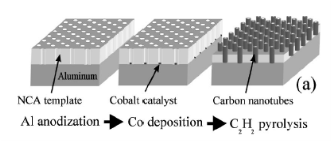
Fig. 1 Schematic of fabrication process. Copyright permission from ref. 13.
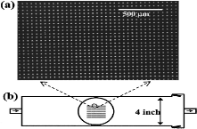
Fig. 2 (a) Optical image of an array of catalyst islands (side length 10 mm) patterned on a wafer using DUV lithography. (b)Diagram of the quartz tube reactor used for growth of annotates. Copyright permission from ref. 14.
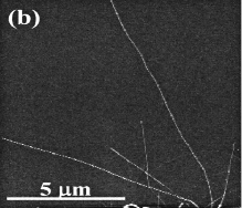
Fig. 3 AFM images of CNTs near catalyst islands on wafer surfaces. Copyright permission from ref. 14.
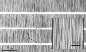
Fig. 4 SEM image of a pattern of perfectly aligned, perfectly linear SWNTs formed by CVD growth on a quartz substrate. The bright horizontal stripes correspond to the regions of iron catalyst. The inset provides a magnified view. These arrays contain 5 SWNTs um-1. Copyright permission from ref. 15.
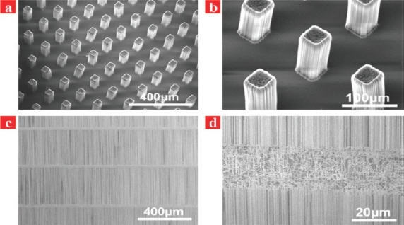
Fig. 5 SEM images of selective growth of vertical aligned islands of CNTs (a, b) and horizontal aligned arrays of CNTs (c, d) on quartz surfaces; (b and d) Higher-resolution SEM images of (a and c), respectively. Copyright permission from ref. 16.
2.2.2 E-beam or ion beam lithography methods
By using a focused ion beam machine, Group of H. B. Peng synthesized directing the controlled growth of SWNTs on specific sites using solid catalyst films. [19] Ali Javey and Hongjie Dai have presented a novel method for patterning individual metallic nanoclusters with tunable and monodisperse sizes down to the 2 nm scale into desired arrays, using an electron-beam lithography technique that has a resolution of 20 nm. [20] Furthermore, they demonstrate chemical vapor deposition synthesis of SWNTs from regular arrays of individual 1.5 nm particles, with the majority of the nanoparticles producing a SWNT at well defined locations, which reaches one of the ultimate goals of SWNT synthesis on surfaces. As clearly illustrated in Fig. 7, arrays of 20-50 nm wells are patterned in 100 nm thick PMMA on Si/ SiO2 (10 nm) substrates. Thin metal films (0.2-2 nm) are deposited by an electron-beam evaporator at a 5-10°angle with respect to the substrate normal. After lift-off and annealing, one or multiple particles per well are formed depending on the well size. Fig. 7C shows us the AFM image of rows of single and multiple Co particles, which provide arrays of metal nanoparticles with diameter below 10 nm for the growth of arrays of carbon nanotubes as shown. In short, it is of the use of e-beam or ion beam to draw a pattern nanometer by nanometer and expose a resist layer allows achieving incredibly small sizes (on the order of 20 nm). This technique, though, is much more expensive and time consuming than photolithography, as the e-beam or ion beam exposure is carried out line- by-line or dot-by-dot, unlike the photolithography by which the whole area can be exposed all at once. It takes orders of magnitude longer to complete the patterning with e-beam or ion beam, so it is therefore difficult to use the e-beam or ion beam lithography for large-scale industry application. Despite its low output and expensive costs, these maskless, direct-patterning methods make it possible for depositing catalyst at specific location for array growing, which offers opportunity for the integration of CNT arrays into electronic devices.
2.2.3 Contact printing patterning
Contact printing is similar to the cover seal in daily life. The poly-siloxane film which has a graphical on surface can be prepared in advance as a seal, and then coated with catalyst solution, drying after the formation of catalyst particles in the seal surface membrane. Polysiloxanne soft board can be also first coated with a catalyst, and then sealed in the silicon substrate which has graphics on surface, leading the protruding micro structure attached to the catalyst. In general, contact printing can be used to pattern small molecule, biomolecules and nanomaterials in the micrometer scale over a large surface area. The low cost and easy processing make it wild accepted. Group of Alan M. Cassellfrom Stanford University have reported their work in 1999, in which they growed single-walled nanotubes parallel to the plane of a silicon substrate directly for the first time.[21] Their growth strategy begins with developing liquid-phase catalyst precursor materials consisting of three general components: inorganic chloride precursors, a removable triblock copolymer serving as the structure-directing agent for the chlorides, and an appropriate alcohol for dissolution of the photo resist patterning and anisotropic etching. The catalyst material is thus transferred to the tower tops and allowed to dry in an oven. The substrate is then heated in air followed by calcinations in air to remove the polymer component. SWNTs are then synthesized on the substrate by chemical vapor deposition. Research group of Lei Ding[22] from Peking University have reported the direct fabrication and uniform patterning of size-tunable Fe2O 3 -xH2O nanoparticles on the SiOx/Si surface. Their method needs neither surface treatment of the stamps nor modification of the substrates with SAMs. Moreover, they are able to pattern nanoparticles with diverse sizes at different locations on one small piece of silicon wafer, which is very convenient in the experiment for the determination of optimum conditions for CVD growth of SWCNTs. As illustrated in Fig. 10, the first step is to “ink” the stamp with the FeCl3-6H2O ethanol solution using a pipette and dry under atmosphere conditions. Then bring the stamp into conformal contact with the substrate for 5 min, and the formed Fe2O3-xH2O nanoparticles transfer onto the silicon oxide substrate; remove the stamp, and a patterned array of Fe2O3-xH2O nanoparticles then forms on the surface. At last the SiOx/Si wafer is put into a tube reactor and the CVD growth of SWCNTs proceeds. Although free standing single-walled carbon nanotubes between silicon towers were grown from catalysts prepared by printing with a flat poly (dimethylsiloxane) (PDMS) stamp, carbon nanotubes on flat substrates are more suitable for nanoelectronics. Group of Gang Gu[23] from Max-Planck-Institute have reported on the single- walled carbon nanotube fabrication on microcontact- printed catalyst patterns that are deposited on electron- transparent, ultrathin silicon nitride membrane substrates. Another innovating work done by group of Weiwei Zhou[24]from University of California, Irvine, in which they used both lithography and Contact Printing method, and successfully obtain patterned, dense, and high-quality SWNT arrays on quartz wafers by CVD of methane. Although, the cantact printing patterning suffered from its unable to grow CNTs arrays at single-tube level, because the achieved catalyst pattern in mostly in micrometer, this unique method hold its own values, such as low cost, easy access and high output.
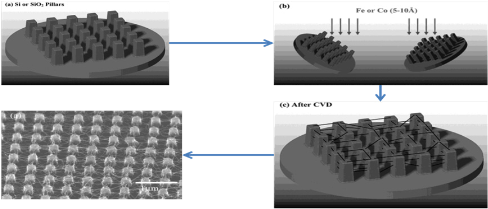
Fig. 6 A general introduction to the process of using X-ray lithography to produce SWNT network and SEM of the final product. Copyright permission from ref. 18.
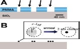
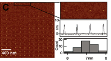
Fig. 7 a and b)Formation of regular arrays of metal clusters down to 2 nm in diameter. c)Patterning of monodispersed 2 and 7 nm Co nanoclusters. Copyright permission from ref. 20.
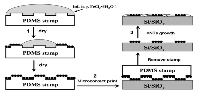
Fig. 8 Schematic Illustration of the Procedures for the Preparation and Patterning of Fe2O3-xH2O Nanoparticles and the Growth of SWCNTs on SiOx/Si Surface. Copyright permission from ref. 22.
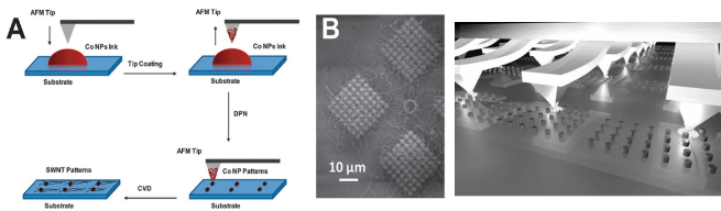
Fig. 9 A. Schematic illustration of the process: AFM tip coating, fabrication of Co NP patterns by DPN, and growth of SWNTs on Co NP patterns. B. SEM images of SWCNTs grown on the DPN-generated Co NP dot arrays on Si/SiOx. Copyright permission from ref. 27. C. Massively parallel DPN with a passive, wire-free, 2D cantilever array. Copyright permission from ref. 28.
2.2.4 Dip-pen nanolithography patterning
In 1999, Piner, R. D.[25] reported the invention of dip- pen nanolithography, which was a significant departure in strategy for using a scanning probe microscope to pattern surfaces. With DPN, molecules that serve as inks are coated on an AFM tip and transported to the surface by engaging the tip and moving it over the surface. DPN also utilizes the water meniscus that naturally forms at the point-of-contact between tip and surface to help control ink transport.[26] Group of Bing Li[27]from Nanyang Technological University report a straight forward method using DPN to generate patterns of cobalt nanoparticles with feature sizes ranging from micrometers down to sub-70 nm. They demonstrated that the DPN-generated Co NP patterns can be used as catalytic templates for growing SWCNTs through chemical vapor deposition (Fig. 9. A). After the CVD process, uniform and high-density SWCNTs were grown on the patterned area, as shown in Fig. 9. One of the main challenges is the development of DPN pertains to throughput. Efforts to increase the throughput of scanning probe lithographies through the use of “multiple pens” cantilever arrays have been extensive. Group of Khalid Salacity [28] from Northwestern University have described a solution to DPN parallelization through the development, fabrication, and use of a novel 55000-pen two-dimensional array to pattern gold substrates with sub-100-nm resolution over square centimeter areas (Fig. 9 C). Furthermore, it has been shown that this approach can be scaled to fabricate an array with as many as 1 million pens that occupy -20 cm2. Also the work suggests that, in the near future, very large-area nanostructure duplication tools based upon sheets of cantilevers will be possible in the context of DPN. In 2008, group of Fenway Hue [29] from Northwestern University published their work in science, in which they reported the development of polymer pen lithography, a low-cost, cantilever-free lithographic approach that, thus far, allows a digitized pattern to be printed at spot sizes ranging from 90 nm to hundreds of mm simply by changing the force and time over which the ink is delivered. They have made and demonstrated patterning capabilities with arrays with as many as ~11,000,000 pens. All of the pens are remarkably uniform in size and shape, with an average tip radius of about 70 nm (Fig. 10 C). The glass support and thin backing layer significantly improve the uniformity of the polymer pen array over large areas, to date up to an entire 3-inch wafer surface (Fig. 10 B). When the sharp tips of the polymer pens are brought in contact with a substrate, ink is delivered at the points of contact Fig. 10 A. Integration of individual nanoparticles into desired spatial arrangements over large areas is a prerequisite for exploiting their unique electrical, optical, and chemical properties. However, positioning single sub-10-nm nanoparticles in a specific location individually on a substrate remains challenging. Group of Jinan Chaia[30] from Northwestern University developed a unique approach: termed scanning probe block copolymer lithography, which enables one to control the growth and position of individual nanoparticles in situ. This technique relies on either dip-pen nanolithography or polymer pen lithography to transfer phase-separating block copolymer inks in the form of 100 or more nanometer features on an underlying substrate. Interestingly, another research using AFM but unlike the above strategy to realize patterned growth of carbon nanotubes was carried out by group of Chien-Chao Chiufrom Nano High-Tech Research Center, Toyota Technological Institute. [31] They provided a novel process to grow CNT selectively on thin Si oxide pattern using AFM nano-oxidation. Selective growth of CNTs was carried out by AFM lithography technique and CVD method, and the procedure is shown in Fig. 11. In general, DPN is a unique scanning probe-based lithographic tool for generating high-resolution patterns of chemical functionality on a range of surfaces. An attractive feature of DPN is that it is both a tool for scientific discovery as well as an engineering advance that allows useful multi-component nanostructures to be printed at a resolution that is superior to any conventional lithographic tool. In an age of nanotechnology, where being able to fabricate nanostructures of a certain composition, size, and shape is essential, DPN in its current state of development is already a tool that will allow for rapid advances in the science and technology of highly miniaturized structures.
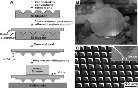
Fig. 10 A. schematic illustration of the polymer pen lithography setup. B. A photograph of an 11-million-pen array. C. Scanning electron microscope image of the polymer pen array. The average tip radius of curvature is 70 nm. Copyright permission from ref. 29.
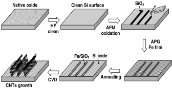
Fig. 11 A schematic of the selective CNT growth on Si oxide pattern made by AFM nano-oxidation. Copyright permission from ref. 31.
2.2.5 Other types of catalyst patterning method
There are some other patterning method developed very recently worth introducing as compensation to the techniques mentioned above ‘‘Needle-Scratching’’ method, a very simple, fast, machine-controlled, environmentally friendly, and nearly no-cost approach, described by the group of Bing Li from Nanyang Technological University, for generating large-area catalyst patterns on Si/SiOx and single-crystal quartz substrates for the growth of densely aligned SWCNT arrays. [32] They show that a high density of well- aligned (up to 10 tubes mm-1) and ultra long SWCNTs (up to 0.5 mm) could be obtained on quartz. Another similar work by group of Bilu Liu[33]from Shenyang National Laboratory for Materials Science suggested that the “scratching” between two Si/SiO2wafers will make the thermally grown SiO2 layer crack and consequently generate some active sites, which have some similarities to the SiO2 film by sputtering deposition, thus facilitating the growth of SWNTs. This “scratching growth” approach is quite simple without using any complex patterning process and could be used for the growth of SWNTs at a precisely predefined position for device fabrication. Group of Hua Zhang has fabricated “all-carbon” electric devices [34] or “all reduced graphene oxide” thin film transistors. [35] Ink-jet printing is familiar as a method of printing text and images onto porous surfaces. Ink-jet printers are also being used to produce arrays of proteins and nucleic acids. [36] Recently, an ink-jet printing technique has attracted interest because of these three advantages: 1) It is possible to fix the position; 2) It can be applied to any substrates, including a flexible one; 3) A minimum amount of ink is consumed, and the pattern is controllable by simply changing the sequence of the nozzle movement. Group of Hiroki Ago have studied the site-selective growth of carbon nanotubes based on ink-jet printing technique through using the Co nanoparticle as ‘‘catalyst ink’’. [37]
2.3 Modulation of CNT array structure
Single CNT structure can be divided into single- walled, double-walled and multi-walled tubes. Currently, the three CNT arrays could be synthesized by modulating the structure and changing the kind and arrangement of catalyst. For the modulation of CNT arrays, different strategies have applied in various methods, but there are a lot of common problems such as controlling the size of the nucleation of catalyst on substrate, composition and process conditions. In the following, modulation of CNT arrays will be discussed in detail.
2.4 Geometry control of CNTS
Briefly, two main mechanisms have been proposed, the first one was called the gas-directed mode [38]while the other was named the surface directed mode[39]. Some other ways were also applied to control the orientation of carbon nanotubes, such as electrical filed orientation. [40] Generally, gas-flow directed mode was used to fabrication of long and aligned carbon nanotubes[38]. It has been observed that a change in heating speed can alter the growth of carbon nanotubes. The growth was further improved in an ultraslow gas flow [41]. The surface directed mode is more complicated, it was found that carbon nanotubes grown on Si (1 0 0)-based surface were aligned in two specific directions, while those grown on Si (1 1 1)-based surface were in three preferred directions. [42] Although the mechanism was quite unclear, a combination of the two modes has been used to achieve special structures. One special complex and coherent geometries of carbon nanotubes, has been made through the combination under a controlled manner. [43]
2.5 The wall number control of CNTs
The controlling of the size of catalyst particles is the key to affect the wall number [44]. However, due to the small diameter of single-walled CNT, the catalyst particles are generally less than a few nanometers [45, 46], so it is necessary to strictly control the catalysts and nuclear size. It was until 2004, there had been reports over the single-walled CNTs arrays [47]. By modulating the size of catalyst particles, Chakrabarti and his group realize the selective growth of single/dual/muli-wall CNT arrays [48]. For CNTs, especially single-welled CNTs, the electrical properties is deeply affected by its intrinsic structures. Therefore the precise control of CNTs felicity through catalyst design and process analysis is very much expected and preferred.
2.6 Length and diameter control of CNTs
For quite a long time, the maximum length of carbon annotates was around several millimeters, until the synthesis of 4-cm-long individual single-walled carbon annotates at a high growth rate [49]. After that, the record was frequently increased from 10 cm [50] to 20 cm [51]. Now, the world record is as long as 40 cm [52]. But, in the case of arrays, for the great complexity, it is still within the micron level. Generally, it is by optimizing the growth conditions and long reaction time to realize the long CNT array growth. As in the case of diameter control, many parameters had been taken into consideration. It has been reported that discrete catalytic nanoparticles with different diameters were obtained by placing controllable numbers of metal atoms into the core of apoferritin, and used for the growth of single-welled carbon nanotubes. It was suggested that the diameters of the nanotubes are determined by the diameters of the catalytical nanoparticles [53]. Temperature is another crucial parameter to control carbon nanotubes diameter. A higher temperature will lead to a larger carbon nanotubes diameter [54]. The gas pressure was also very important in determining the diameter [55].
3. Applications
Interest in the detection of DNA has grown rapidly because of its importance in diagnose and treatment of genetic disease, drug discovery, and anti-bioterrorism efforts. [56] The combination of the unique properties of CNT arrays with DNA hybridization offers the possibility of constructing DNA biosensors with simplicity, high sensitivity and multiplexing. These arrayed carbon annotates can be discretely control the region and density. Additionally, these CNTs structures exhibit high electrical conductivity and quick electronic transfer speed [57- 58], and every individual nanotube can act as a minisize nanostructured electrode with a maximized accessibility for analytes during electrochemical detection. Therefore, using arrayed carbon nanotubes as a novel electrode offers promising prospect for fabricating a sensitive and selective nanoscale DNA analysis system. Several research groups have already begun their attractive research works of fabricating CNTs array-based DNA biosensors. [59–64] Dai et al. employed acetic acid-plasma method to graft active carboxyl groups onto gold-supported aligned carbon nanotubes from tips to sidewalls. Probe oligonucleotide was subsequently covalently attached onto these arrayed nanotubes, and after the hybridization of probe with its FCA (ferrocenecarboxaldehyde) labeled complementary sequence, the authors detected the amperiometeric response of FCA as hybridization signal[61]. This presented DNA biosensor protocol has powerful regeneration ability and high amperiometeric response with 20 times higher than using conventional flat electrode.Wang’s work shows that the higher efficiency of DNA hybridization on CNTs array is mainly resulted from the special structure of self-assembled MWNTs, which offers enough space for target DNA molecules accessing the immobilized DNA probe [62]. Kelley et al. employed two immobilization strategies to selectively immobilize DNA sequences at different sites of MWNTs-COOH. [63] All these CNTs array-based works indicate that arrayed carbon nanotubes electrodes with ordered structure represent a promising new generation electrodes for sensitive sequence-specific DNA diagnoses, and the fabrication of highly automated DNA chips with multiplex nanoelectrode arrays for quick DNA analysis is becoming possible by applying optimized CNTs arrays. Beside the carbon nanotube array-based biosensor, the arrayed CNTs has find its applications in various fields, such as photovoltaic, field emission IR detection, transistors and other classes of electronic devices etc[64- 67].
4. Conclusions
Research and development of CNT arrays provides a new structure for nanomaterials, which has greatly enriched the types and applications of carbon materials. The various applications have been the main driving force in promoting CNT array study. With all those insightful findings mentioned above, it is reasonable to see the electronic devices with desirable structure and properties realized using CNT arrays. Still, further research and development both theoretically and experimentally on precisely controlling of growth and modulating of CNT arrays are very much needed.
References
1. P. G. Collins, A. Zettl, H. Bando, A. Thess, and R. E. Smalley. Nanotube nanodevice. Science. 1997; 278: 100-102. http://dx.doi.org/10.1126/science.278.5335.100
2. S.J. Tans, A.R.M. Vershuerent and C. Dekker. Room-temperature transistor based on a single carbon nanotube. Nature 1998; 393: 49- 52. http://dx.doi.org/10.1038/29954
3. Iijima S.Helical. Microtubules of graphitic carbon. Nature 1991, 354, 56-71.http://dx.doi.org/10.1038/354056a0
4. Theses A,Lee R,Nikolaev P, et al. Crystalline ropes of metallic carbon nanotubes.Science.1996; 273:483-488.http://dx.doi. org/10.1126/science.273.5274.483
5. Franklin, NR; Li, Y.; Chen, RJ; Jared, A.; Dai, H. Patterned growth of single-walled carbon nanotubes on full 4-inch wafers. Appl. Phys. Lett. 2001; 79:4571-4573.http://dx.doi.org/10.1063/1.1429294
6. A. Jorio, G. Dresselhaus and M.S. Dresselhaus, Carbon Nanotubes: Advanced Topics in the Synthesis, Structure Properties and Applications, Spinger, 2008.
7. Jensen K, et al. Chemical Vapor Deposition in Microelectronics Processing: Chemical Engineering Aspects. American Chemical Society. 1989, chapter 1, pp 1-33.
8. Li w Z, Xie S S, Qian L X, et al. Large—scale synthesis of aligned carbon namotubes. Scieace,1996,274, 1701—1703.
9. Y. Yan, M. B. Chan-Park and Q. Zhang. Advances in carbon- nanotube assembly. Small, 2007, 3, 24-42. http://dx.doi.org/10.1002/ smll.200600354
10. J. Liu, A. G. Rinzler, H. Dai, J. H. Hafner, R. K. Bradley, P. J. Boul, A. Lu, T. Iverson, K. Shelimov, C. B. Huffman, F. RodriguezMacias, Y.-S. Shon, T. R. Lee, D. T. Colbert and R. E. Smalley. Fullerene pipes. Science. 1998; 280:1253-1255.http://dx.doi.org/10.1126/ science.280.5367.1253
11. V. C. Moore, M. S. Strano, E. H. Haroz, R. H. Hauge, R. E. Smalley, J. Schmidt and Y. Talmon.individually suspended single-walled carbon nanotubes in various surfactants. Nano Lett. 2003; 3:1379- 1382.http://dx.doi.org/10.1021/nl034524j
12. Yiu. W. C, Au. F. C. K, Ding. J. X, Lee. C. S, Lee. S. T. Electrical properties of zinc oxide nanowires and intramolecular p-n junctions. Appl. Phys. Lett. 2003, 83, 3168-3170.
13. J. Li, C. Papadopoulous, J. M. Xu. Highly ordered carbon nanotube arrays for electronics applications. Appl. Phys. Lett. 1999; 75:367- 369.
14. Franklin NR, Li Y, Chen RJ, Jared A, Dai H. Patterned growth of single-walled carbon nanotubes on full 4-inch wafers. Appl. Phys. Lett. 2001; 79:4571-4573.http://dx.doi.org/10.1063/1.1429 294
15. Song Jun Kang, Cookson Koalas, Tanner Ouzel, Moon sub Shim, Nina Pimparkar, Muhammad A. Alma, Slave V. Rot Kin and John A. Rogers. High-performance electronics using dense, perfectly aligned arrays of single-walled carbon nanotubes. Nature Nanotechnology 2007; 2:230-236.http://dx.doi.org/10.1038/ nnano.2007.77
16. Weise Zhou, Lei Ding, Sung woo Yang, and Jibe Liu. Orthogonal Orientation Control of Carbon Nanotube Growth. AM. CHEM. SOC. 2010; 132:336–341.
17. Suck Won Hong, Tony Banks, and John A. Rogers. Improved Density in Aligned Arrays of Single-Walled Carbon Nanotubes by Sequential Chemical Vapor Deposition on Quartz. Adv. Mater. 2010; 22:1826-1830.http://dx.doi.org/10.1002/adma.200903238
18. Yung Joon Jung, Yoshikazu Homma,Toshio Ogino,Yoshihiro Kobayashi,Daisuke Takagi, Bingqing Wei, Robert Vajtai, and Pulickel M. Ajayan. High-Density, Large-Area Single-Walled Carbon Nanotube Networks on Nanoscale Patterned Substrates. J. Phys. Chem. B 2003; 107:6859-6864. http://dx.doi.org/10.1021/ jp0346514
19. H. B. Peng, T. G. Ristroph, G. M. Schurmann, G. M. King, J. Yoon et al. Patterned growth of single-walled carbon nanotube arrays from a vapor deposited Fe catalyst. Appl. Phys. Lett. 2003; 83: 4238-4240.http://dx.doi.org/10.1063/1.1627935
20. Ali Javey and Hongjie Dai. Regular Arrays of 2 nm Metal Nanoparticles for Deterministic Synthesis of Nanomaterials. J. AM. CHEM. SOC. 2005, 127, 11942-11943.http://dx.doi.org/10.1021/ ja0536668
21. Alan M. Cassell, Nathan R. Franklin,Thomas W. Tombler, Emory M. Chan,Jie Han, and Hongjie Da. Directed Growth of Free- Standing Single-Walled Carbon Nanotubes. J. Am. Chem. Soc. 1999; 121:7975-7976.
22. Lei Ding, Weise Zhou, Hailing Chu, Hong Jin, Yan hang, and Yan Li. Direct Preparation and Patterning of Iron Oxide Nanoparticles via Microcontact Printing on Silicon Wafers for the Growth of Single-Walled Carbon Nanotubes. Chem. Mater. 2006; 18:4109- 4114.http://dx.doi.org/10.1021/cm061122e
23. Gang Gu, Günther Philipp, Xiaochun Wu, Marko Burghard, Alexander M. Bittner, and Siegmar Roth. Growth of Single-Walled Carbon Nanotubes from Microcontact-Printed Catalyst Patterns on Thin Si3N4 Membranes. Adv. Funct. Mater. 2001, 11, 295-298. http://dx.doi.org/10.1002/1616-3028(200108)11:4<295::AID- ADFM295>3.0.CO;2-2
24. Weiwei Zhou, Christopher Rutherglen and Peter J. Burke. Wafer Scale Synthesis of Dense Aligned Arrays of Single-Walled Carbon Nanotubes. Nano Res .2008, 1,158- 165.http://dx.doi.org/10.1007/ s12274-008-8012-9
25. Piner R D, Zhu J, Xu F, Hong S H, Mirkin C A. “Dip-Pen” Nanolithography. Science 1999; 283:661–663.
26. Ginger, D. S.; Zhang, H.; Mirkin, C. A.The Evolution of Dip-Pen Nanolithography. Angew. Chem. Int. Ed. 2004; 43:30–45.http:// dx.doi.org/10.1002/anie.200300608
27. Bing Li, Chin Food Go, Xiaozhu Zhou, Gang Lu, Hosea Tantung, Yangon Chen, Can Due, Freddy Y. C. Boy, and Hue Hang. Patterning Colloidal Metal Nanoparticles for Controlled Growth of Carbon Nanotubes. Adv. Mater. 2008, 20, 4873–4878. http://dx.doi.org/10.1002/adma.200802306
28. Khalid Salacity, Yahooing Wang, Joseph Fragile, Rafael A. Vega, Chang Liu, and Chad A. Massively Parallel Dip–Pen Nanolithography with 55000-Pen Two-Dimensional Arrays. Marking, Anew. Chem. Int. Ed. 2006; 45:7220 –7223.
29. Fenway Hue, Fijian Zheng, Gengfeng Zhen, Louise R. Giam, Hua Zhang, Chad A. Marking. Polymer Pen Lithography. SCIENCE, 2008, 321, 1658-1660.http://dx.doi.org/10.1126/science.1162193
30. Jinan Chai, Fengwei Hue, Fijian Zhen, Louise R. Guam, Woo young Shim, and Chad A. Marking. PS canning probe block copolymer lithography. NAS, 2010; 107: 20202–20206. http://dx.doi.org/10.1073/pnas.1014892107
31. Chien-Chao Chiu, Masamichi Yoshimura, Kazuyuki Ueda. Patterned growth of carbon nanotubes through AFM nano- oxidation. Diamond Relat. Mater . 2009 ; 18 : 355 - 359. http://dx.doi.org/10.1016/j.diamond.2008.09.010
32. Bing Li, Xiehong Cao, Xiao Huang, Gang Lu, Yizhong Huang, Chin Foo Goh, Freddy Y. C. Boey, and Hua hang. Facile ‘‘Needle- Scratching’’ Method for Fast Catalyst Patterns Used for Large-Scale Growth of Densely Aligned Single-Walled Carbon-Nanotube Arrays. Small 2009; 5:2061–2065.http://dx.doi.org/10.1002/ smll.200900654
33. Bilu Liu, Wencai Ren, Libo Gao, Shisheng Li, Songfeng Pei, Chang Liu, Chuanbin Jiang, and Hui-Ming Cheng. Metal-Catalyst-Free Growth of Single-Walled Carbon Nanotubes. J. AM. CHEM. SOC. 2009, 131, 2082–2083.http://dx.doi.org/10.1021/ja8093907
34. B. Li, X. Cao, H. G. Ong, J. W. Cheah, X. Zhou, Z. Yin, H. Li, J. Wang, F. Boey, W. Huang and H. Zhang . All-Carbon Electronic Devices Fabricated by Directly Grown Single-Walled Carbon Nanotubes on Reduced Graphene Oxide Electrodes. Adv. Mater. 2010, 22, 3058-3061.http://dx.doi.org/10.1002/adma.201000736
35. Q. Y. He, S. X. Wu, S. Gao, X. H. Cao, Z. Y. Yin, H. Li, P. Chen and H. Zhang. Transparent, Flexible, All-Reduced Graphene Oxide Thin Film Transistors. ACS Nano 2011; 5:5038-5044.http://dx.doi. org/10.1021/nn201118c
36. Paul Calvert. Inkjet Printing for Materials and Devices. Chem. Mater. 2001; 13:3299-3305.http://dx.doi.org/10.1021/cm0101632
37. Hiroki Ago, Kazuhiro Murata, Motoo Yumura, Junko Yotani, and Sashiro Uemura. Ink-jet printing of nanoparticle catalyst for site-selective carbon nanotube growth. Appl. Phys. Lett.2003; 82:811-813.http://dx.doi.org/10.1063/1.1540726
38. Su M, Li Y, Maynor B, Buldum A, Lu JP, Liu J. Lattice-oriented growth of single-walled carbon nanotubes. Phys Chem B 2000; 104: 6505–6508.http://dx.doi.org/10.1021/jp0012404
39. Huang SM, Woodson M, Smalley R, Liu J. Growth mechanism of oriented long single walled carbon nanotubes using ‘‘fastheating’’ chemical vapor deposition process. Nano Lett 2004; 4:1025–1028. http://dx.doi.org/10.1021/nl049691d
40. Zhang YG, Chang AL, Cao J, Wang Q, Kim W, Li YM, et al. Electric-field-directed growth of aligned single-walled carbon nanotubes. Appl Phys Lett. 2001; 79:3155–3157.http://dx.doi. org/10.1063/1.1415412
41. Jin Z, Chu HB, Wang JY, Hong JX, Tan WC, Li Y. Ultralow feeding gas flow guiding growth of large-scale horizontally aligned single- walled carbon nanotube arrays. Nano Lett. 2007; 7:2073–2079. http://dx.doi.org/10.1021/nl070980m
42. Su M, Li Y, Maynor B, Buldum A, Lu JP, Liu J. Lattice-oriented growth of single-walled carbon nanotubes. J Phys Chem B. 2000; 104: 6505–6508.http://dx.doi.org/10.1021/jp0012404
43. Geblinger N, Ismach A, Joselevich E. Self-organized nanotube serpentines. Nat Nanotechnol. 2008; 3:195–200.http://dx.doi. org/10.1038/nnano.2008.59
44. Qiao W Z, Liu T, Wei F. et al Carboll nanotmies containing iron and molybdenum particles as a catalyst for methane decomposition. Carbon,2003, 41, 846-848.http://dx.doi.org/10.1016/S0008- 6223(02)00422-0
45. Niag G Q,Wei F,Wen Q,el al Improvement of Fe/MgO catalystsy calcination for the growth of single-and double-walled carbon nanotabes. Journal of Physical Chemistry B. 2006; 110:120l-1205.
46. Ning G Q,Liu Y,Wei F,at a1.Porous and lamella-like Fe/MgO catalysts prepared under hydrothermal conditions for high yield synthesis of double—walled nanotubes. Journal of Physical Chemistry C. 2007; 111: 1969-1975.
47. Hata K,Futaba D N,Mizuno K,et d.Water-assisted highly efficient synthesis of impurity-free single-walled carbon nanotubes. Science, 2004; 306:1362-1364.
48. Chakrabaai S., Kume H., Pan L.J. et al. Number of walls controlled synthesis of millimeter-long vertically aligned brushlike carbon nanotubes. The Joumal of Physical Chemistry C. 2007; 11l:1929- 1934.http://dx.doi.org/10.1021/jp0666986
49. Zheng LX, O’Connell MJ, Doorn SK, Liao XZ, Zhao YH, Akhadov EA, et al. Ultra-long single-wall carbon nanotubes. Nat Mater. 2004; 3:673–676.http://dx.doi.org/10.1038/nmat1216
50. Wen Q, Qian WZ, Nie JQ, Cao AY, Ning GQ, Wang Y. et al. 100 mm long, semiconducting triple-walled carbon nanotubes. Adv Mater, 2010; 22:1867–1871. http://dx.doi.org/10.1002/ adma.200902746
51. Wen Q, Qian WZ, Zhang RF, Wang YR, Tan PH, Nie JQ, et al. Growing 20 cm long DWNTs/TWNTs at a rapid growth rate of 80–90 lm/s. Chem Mater. 2010; 22: 1294–1296.http://dx.doi. org/10.1021/cm903866z
52. Croci M, Arfaoui I, Stockli T, Chatelain A, Bonard JM. A fully sealed luminescent tube based on carbon nanotube field emission. Microelectron J, 2004, 35, 329–336.http://dx.doi.org/10.1016/ j.mejo.2003.07.003
53. Li YM, Kim W, Zhang YG, Rolandi M, Wang DW, Dai HJ. Growth of single-walled carbon nanotubes from discrete catalytic nanoparticles of various sizes. J Phys Chem B. 2001; 105:11424– 11431. http://dx.doi.org/10.1021/jp012085b
54. Yao YG, Li QW, Zhang J, Liu R, Jiao LY, Zhu YT, et al. Temperature-mediated growth of single-walled carbonnanotube intramolecular junctions. Nat Mater. 2007; 6: 283–286. http://dx.doi.org/10.1038/nmat1865
55. Hiraoka T, Bandow S, Shinohara H, Iijima S. Control on the diameter of single-walled carbon nanotubes by changing the pressure in floating catalyst CVD. Carbon, 2006; 44:1853–1859. http://dx.doi.org/10.1016/j.carbon.2006.03.024
56. A. Sassolas, D.L. Leca-Bouvier, L.J. Blim. DNA Biosensors and Microarrays. Chem. Rev. 2008; 108:109-139.http://dx.doi. org/10.1021/cr0684467
57. Dresselhaus MS, Dresselhaus G, Avouris P. Carbon nanotubes: synthesis, structure, properties, and applications. Springer, 2001.
58. Saito R, Dresselhaus G, Dresselhaus M S.Physical properties of carbon nanotubes, Imperial College Press, 1998.
59. Li J, Ng H T, Cassell A, Fan W, Chen H, Ye Q, Koehne J, Han J, Meyyappan M. Carbon Nanotube Nanoelectrode Array for Ultrasensitive DNA Detection. Nano Lett. 2003, 3, 597-602. http://dx.doi.org/10.1021/nl0340677
60. Koehne J, Li J, Cassell A M, Chen H, Ye Q, Ng H T, Han J, Meyyappan M.The fabrication and electrochemical characterization of carbon nanotube nanoelectrode arrays. J Materials Chemistry 2004, 14, 676 -680.http://dx.doi.org/10.1039/b311728f
61. He P G, Dai LM. Aligned carbon nanotube-DNA electrochemical sensors. Chem Commun. 3, 348-349.
62. S G Wang, Ruili Wang, Sellin P J, Zhang Q. DNA biosensors based on self-assembled carbon nanotubes. Biochem Biophys Res Commu, 2004, 325, 1433-1437.http://dx.doi.org/10.1016/ j.bbrc.2004.10.188
63. Taft B J, Lazareck A D, Withey G D, Yin A J, Xu J M, Kelley. Site- Specific Assembly of DNA and Appended Cargo on Arrayed Carbon Nanotubes. J. Am. Chem. Soc. 2004; 126:12750–12751. http://dx.doi.org/10.1021/ja045543d
64. R.E. Camacho, A.R. Morgan, M.C. Flores, T.A. McLeod, V.S. Kumsomboone, B.J. Mordecai,R. Bhattacharjea, W. Tong, B.K. Wagner, J.D. Flicker, S.P. Turano, and W.J. Ready. Carbon Nanotube Arrays for Photovoltaic Applications. JOM Journal of the Minerals, Metals and Materials Society. 2007; 59:39-42.http:// dx.doi.org/10.1007/s11837-007-0037-0
65. W. I. Milne, K. B. K. Teo, G. A. J. Amaratunga, P. Legagneux, L. Gangloff, J.-P. Schnell, V. Semet, V. Thien Binhc and O. Groening. Carbon nanotubes as field emission sources. J. Mater. Chem. 2004, 14, 933–943.
66. J.M. XU. Highly ordered carbon nanotubes arrays and IR detection. Infrared Physics & Technology 2001, 42, 485-491. http://dx.doi.org/10.1016/S1350-4495(01)00102-5
67. Song Jun Kang, Coskun Kocabas, Taner Ozel, Moonsub Shim, Ninda Pimparkar, Muhammda A. Alam, SlavaV. Rotkin and John A Rogers. High-performance electronics using dense, perfectly aligned arrays of single-walled carbon nanotubes. Science. 2007; 2: 230-236.
Copyright:(c) 2012 Huiyang Liu, et al. This is an open- access article distributed under the terms of the Creative Commons Attribution License, which permits unrestricted use, distribution, and reproduction in any medium, provided the original author and source are credited.

|
Nano Biomedicine and Engineering. Copyright © Shanghai Jiao Tong University Press |
 |