Research Article
Sensitivity of Cadmium Sulfide under the Influence of Both Substrate Temperature and Gas Operation
Ehssan Salah Hassan 1, Zaid Saud Razzaq 2, Huda Ashur Shati Qutbi 3, Sami Salman Chiad 4, Nadir Fadhil Habubi 4, Khalid Haneen Abass 5 *
1 Department of Physics, College of Science, Mustansiriyah University, Baghdad, Iraq.
2 Department of Sciences, Faculty of Basic Education, Al-Muthanna University, Al Muthanna, Iraq.
3 Physiology and Medical Physics Department, College of Medicine, University of Wasit, Wasit, Iraq.
4 Department of Physics, College of Education, Mustansiriyah University, Baghdad, Iraq.
5 Department of Physics, College of Education for Pure Sciences, University of Babylon, Iraq.
*Corresponding author E-mail: pure.khalid.haneen@uobabylon.edu.iq
Received: May 4, 2021; Accepted: Dec. 2, 2021; Published: Dec. 16, 2021
Citation: Ehssan Salah Hassan, Zaid Saud Razzaq, Huda Ashur Shati Qutbi, Sami Salman Chiad, Nadir Fadhil Habubi, and Khalid Haneen Abass, Sensitivity of Cadmium Sulfide under the Influence of Both Substrate Temperature and Gas Operation. Nano Biomed. Eng., 2021, 13(4): 425-432.
DOI: 10.5101/nbe.v13i4.p425-432.
Abstract
The importance of this research is to study the effect of changing the temperature at the same time on each of the prepared samples and during the gas sensing processes, the effects of substrate temperature Ts were investigated after precipitation by the microstructural and optical characteristics of cadmium sulfide using thermal spraying method with different temperatures of (300, 400, and 500) ºC. The structural investigations of these films were studied, showing that the increases in substrate temperature were shown cubic and hexagonal phases according to ICDD card no. (21-0929) and (43-0989). The dramatic change occurred at 500 oC in changing the phase from hexagonal to a cubic structure. XRD exhibits a dominant plane at (200) for different substrate temperatures. Optical transmittance, absorption coefficient, and energy gap values were calculated by UV/VIS spectrophotometer. These results showed that the band gap values decreased with increasing substrate temperature. The gas sensitivity was tested for NO2 gas at several working temperatures from 175 ºC to 250 ºC, and various gas concentrations from 150 ppm to 200 ppm and found that the sensitivity increase with increasing both the operating temperature and gas concentration for a Ts at 500 ºC which offer also the best crystallization the best sensitivity at an operating temperature of 175 oC is 75% at a gas concentration of 150 ppm.
Keywords: SPM, Substrate temperature, Hexagonal phase, Cubic phase, Sensitivity, Recovery and response time
Introduction
The optical and structural characteristics of cadmium sulfide CdS films grown by chemical spraying method SPM is dependent on several factors, such as material concentration involved in the reaction [1], the PH [2], the thickness of the resulting deposited film [3]. In chemical spraying processes, film development processes are performed either by condensing ion with ion, or by adsorbing the colloidal solution from the surface of the substrate [4]. Many methods are used for the preparation of cadmium sulfide, including vacuum thermal evaporation [5], RF and DC sputtering [6], screen printing [7], chemical bath deposition [8], Spin coated [9], hot injection method [10], but among these methods chemical spraying was more affordable and easy to prepare thin films from chemical reactions in addition the grown films were homogeneous and high adhesion. [11-13]. Optical characteristics like permeability, absorption and energy gap values are important for gas sensing applications [14]. Gas sensor is very important applications in science in which cadmium sulfate is used mainly single or polycrystalline. Cadmium sulfide has been widely used in factories, scientific laboratories, mines or houses, for its unique electrical and optical properties in providing high efficiency and long running life due to their stable performance, high-efficiency and low cost, and were utilized for large area terrestrial applications [15]. In the present study, NO2 is considered as a dangerous gas that is emitted from the burnings of car engines exhaust, plants, furnaces and home heaters [16]. Thus, there is a high importance in developing sensors that are small in size, quick in response, with long-lifetime and adequate sensitivity to detect NO2 even in low concentrations [17]. CdS films as a sensor to study the interaction of oxygen gas [18]. study the performance of CdS on H2S gas [19]. alcohol gas by CdS sensor [20]. CdS films to detect NO2 gas [21]. the optical, structural and sensing characteristics of CdS were examined and the results are discussed.
Experimental
Cadmium sulfide films are prepared utilizing chemical spray pyrolysis technique. CdCl2 supplied from (BDH chemical) was used as a source of cadmium whereas theories (NH2CSNH2) supplied from (BDH Chemicals) was employed to obtain sulfur on the saturated solution CdCl2 with deionized water in 1:1 volume proportion. This solution was sprayed onto the preheated substrate at a different temperature of 300ºC, 400ºC and 500ºC. The optimum condition to obtain homogenous thin film free from any notable crack arrives at the following; Nitrogen was the carrier gas, distance between nozzle and substrate was 28.0cm, the spray rate was 8 ml/ min. CdS thin film thickness is measured by gravimetric method. All as deposited CdS thin films have a thickness of 300 ± 30 nm. UV. A UV-Visible double spectrophotometer in wavelength range of (300nm – 900 nm) was used to determine the value of transmittance and absorbance spectra.
Result and discussion
Structural and morphological
Fig. 1 exhibits the XRD patterns of CdS films. CdS films at low substrate temperature 300ᵒC and 400ᵒC exist in polycrystalline hexagonal structure according to ICDD no. 10-0454 [20]. The preferred reflection at 300oC and 400oC is (020) plane at 2θ=36.34ᵒ for hexagonal phase. Besides, many secondary reflections at (001), (110), (021), (121), (102) and (220) for hexagonal phase at angles 2θ=26.18ᵒ, 31.60ᵒ, 45.32ᵒ, 53.12ᵒ, 60ᵒ and 66.31ᵒ were observed. At the substrate temperature of 500oC the preferred reflection was changing from (020) to (200) plane at 2θ=32.43ᵒ and to the cubic according to ICDD n. 06-0314. This level makeover from hexagonal to cubic is formerly identified for chemically deposited CdS films. [23-24]. It is worth noting here that the temperature 400 ᵒC represented the turning point from the cubic phase to the hexagonal at the reflection of (200) at the angle of 2θ= 32.43ᵒ and as shown in the inset figures attached to Fig. 1 with several secondary reflections at (111), (220) and (400) at angles 2θ= 28.31, 47.87 and 68.12. This level makeover from hexagonal to cubic is formerly identified for chemically deposited CdS films. The regular (200) reflection at 2θ = 32.43ᵒ recycled to analyze the crystallite sizes from the XRD decoration, as anticipated, growing the substrate temperature effects an improvement of Bragg reflections, indicating an increase in film’s crystallinity. Also, crystallite size was conducted with the use of Scherer’s formula [25]:
![]()
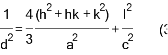
In which K is the shape factor, β representing full-width at the half maximum FWHM related to Bragg reflection within considerations in radians, λ is the wavelength of X-ray, and θ representing Bragg angle. Equation (1) is applied for calculating the crystallite sizes (D) with the use of K = 0.9, while the lattice parameter values are calculated utilizing equations [25]:
![]()
The crystallite size that is related to Ts of (300ºC) is 20.42 nm and was increase to (26 nm) with the increase in Ts to 500 ºC. The microstrain (ε) is obtained by equation (4) resulted throughout the film growth and is going to be elevated from compression or stretching in a lattice. Besides, ε reduction resulting from changing the atom’s displacement in terms of their reference lattice position. Fig 2(b) is showing that there will be a decrease in ε with the increase in Ts, which might be caused by the increase in film’s crystallinity. Besides, the dislocation density (δ) can be defined as a number of dislocation per unit volume utilizing equation (5). Fig 2(c) is showing a decrease in dislocation density with the increase in substrate Ts. The results related to ε eq. (4) as well as the δ values are indicated in Table 1 [26]:
![]()
![]()
Table 1 lists the calculated structural parameters. where the application of Gaussian for a process of Fit for reflection preferred as shown in Fig. 2(d) and (e), which gives high precision values. Fig. 3 shows Energy Dispersive Spectrometry EDS, which gives a precise illustration of the elements that make up the membrane by weight ratios of wt% and atomic atoms at%. From the figure we note the emission spectrum Oxygen spectrum (Kα = 0.50 keV and the cadmium spectrum at Kα = 2.75 keV, Lα = 3.1 keV, Mα = 3.31 keV, and Mα = 3.99 keV. And the sulfur spectrum of Kα = 2.52 eV. The AFM micrographs of CdS with different substrate temperature films (Fig. 4) exhibits that the grain distribution is not even over all areas. However, Fig. 4 shows the presence of smooth and bright regions. In Fig. 4(g) we notice that the average diameter is larger and resembles the vertical growth and more closely the density of nanoparticles on the shape of vertical rods on the surface of the nanostructured film with an average diameter of (20 -30) nm and the height (80 – 120) nm compared to the Fig. 4(d) in which the bright areas are (with little growth) with less intensity or in Fig. 4(h) as the substrate temperature Increasing from 300oC to 400oC. The reason for the difference in crystallite size that calculated from X-Ray diffraction pattern and the mean grain size that measured by AFM is that the XRD deals with wavelengths that do not exceed the λ = 1.5432 Å, that is, it measures units at the level of the unit cell while the AFM deal with a group of unit cells and grain boundary, which consists of one atom or more. As indicated in Figures (4a, b and c) the rate of average diameter will be increased with the increase in substrate temperature accompanied with RMS as well as roughness average that decreases when the substrate temperature increase.
Table 1 Structural data of CdS at various Ts by SPM)
|
Ts ºC |
(hkl) Plane |
2theta (Deg.) |
Lattice constant (Å) |
FWHM (Rad) |
Crystallite size D (nm) |
Micro-strain (lineˉ².mˉ1)× 10ˉ3 |
Density of Dislocation (δ) (line.mˉ²)×1015 |
|
|
300 |
(020) |
36.34 |
a |
c |
0.37 |
20.42 |
1.532 |
2.397 |
|
3.55 |
3.67 |
|||||||
|
400 |
(020) |
35.87 |
a |
c |
0.33 |
23.140 |
1.381 |
1.867 |
|
3.56 |
3.65 |
|||||||
|
500 |
(200) |
32.43 |
a |
0.29 |
26.08 |
1.202 |
1.469 |
|
|
5.34 |
||||||||
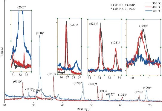
Fig. 1 XRD pattern of CdS with different substrate temperatures by SPM.
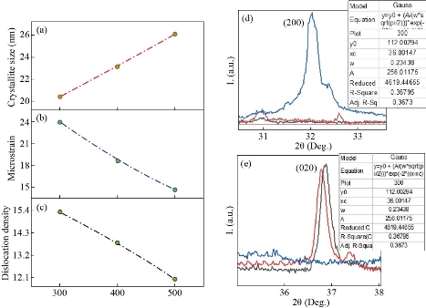
Fig. 2 The variation of (a) size of the crystallite, (b) micro-strain and (c) density of dislocation (d) and (e) FWHM for the preferred diffraction CdS films with the substrate temperature.
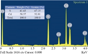
Fig. 3 Energy Dispersive Spectrometry for the preferred diffraction CdS films with the substrate temperature.
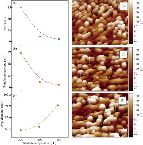
Fig. 4 AFM, 3-D image of CdS nanostructured film (a)-(c) RMS, Roughness Average and Avg. Diameter, (d) 300 oC, (h) 400 oC and (g) 500 oC.
Transmittance and absorption coefficient
Fig. 5 represents the transmittance spectra values as the function of wavelength of cadmium sulfide CdS deposited by chemical spray pyrolysis. From transmittance spectra, values of the transmittance decrease with the increase of the substrate temperature where it was 90% at Ts of 300oC and decreased to 86% and then 83% with a Ts rise to 400oC and 500oC respectively. It may be due to changes in the structural and morphological characteristics of surface transformation in the phase from the hexagonal to the cubic, and the increase in crystal size. Fig. (5-b) representing the values related to absorption coefficient deducing that the band gap type was direct since such values were more than 105 [27]. Also, their dependence in drawing the relations between the values of photon energy (hν) as well as (αhν)2 as in Fig (5-c), in which the band gap value was evaluated via extrapolation of the straight line of the plot of (αhν)2 vs. the energy of the photon, which is observed to decrease as the base temperature increases.
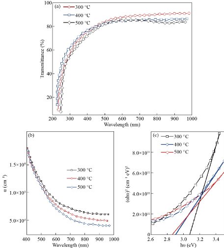
Fig. 5 (a) Transmittance as function to the wave-length for CdS by (SPM). (b) Absorption coefficient. (c) Band gap.
Gas sensing properties
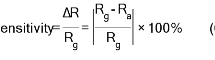
The gas sensing characteristics of nanostructured CdS films of that prepared at 500oC for a variety of gas concentrations of NO2 as oxidized gas are examined as a function of various operation time. Fig (6-a) is showing the dynamic resistance changes related to the nanostructured CdS films which are prepared at a temperature of 500oC through (SPM), exposure to various NO2 gas concentrations (150, 200 as well as 250) ppm. It is indicated that the lowest resistance is for samples at 175oC and increasing due to the highest roughness acquired from the AFM analysis as well as the n-type semiconductor performance [28] also the film’s resistance will be increased with an increase in NO2 concentrations in the chamber [29], this might be justified as electrons have been taken from ionized donors via conduction band, also the density which is related to majority charge carriers (electrons) at gas film surface interface was reduced. In addition, this will result in increasing the potential barrier for electrons with an increase in oxygen ion density on the surface. Also, the potential barrier and depletion layer are leading to an increase in the value of electrical resistivity, such value is depending on the concentrations of the adsorbed oxygen ions on the surface [29]. The sensitivity might be estimated from equation (6) and plotted as a function of operating temperature as seen in Fig (6-c).
The sensitivity percentage value of CdS films of NO2 gas with various operating temperatures is increased with the increase in film’s operating temperatures and highest value of sensitivity has been 75% for 250ppm gas concentrations of NO2 acquired from the film of 500oC substrate temperature at operation temperature 250oC. Besides, the sensitivity related to metal oxide semiconductor sensor was majorly specified via interactions between sensor’s surface and the target gas [30]. Interactions between sensor surface and adsorbed gases is stronger as the surface area of materials showed in AFM measurements becomes greater. Figures (6-d) and (6-e) show the response time as well as recovery time, respectively, which might be directly estimated from Fig. 5(a), and plotted as a function of substrate temperature. Fig. 6(d) is showing the response time, which is decreasing from (15 to about 120) sec. The increase in substrate temperature could be attributed to the large availability related to vacant sites on the thin films for gas adsorption [31]. While Fig. 6(e) shows a slight decrease in the range that does not exceed 20 seconds for all samples. As the substrate temperature increases, thus increasing because of the sensor’s saturation via target gas, also the variations in the structural characteristics might occur through operating temperature.
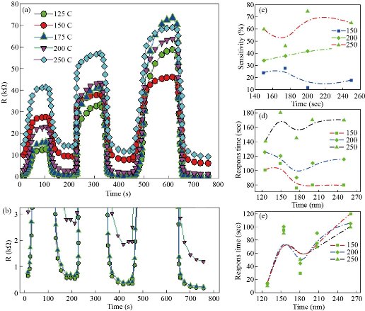
Fig. 6 (a) Dynamic Resistance Change of CdS Film at a substrate temperature of 500oC for Various NO2 Gas Concentrations and Various Operating Temperatures. (b) The clip is magnified with small values of resistance and relative to the X-Axis. (c) Sensitivity as a function to substrate temperature. (d) Recovery time as a substrate temperature function, (e) Response time as a function of substrate temperature
Conclusions
The films were prepared within various substrate temperatures, it is indicated that the films are polycrystalline with hexagonal phase at a temperature of 300 oC and start a very simple change at 400oC, but at 500oC of substrate temperature turns from the hexagonal to the cubic phase 100% and the prevailing orientation changes from (020) plane to (200) plane and increased particle size and improved crystallization. The selected model for the measurement of the gas sensor at the substrate temperature 500 oC was the best sensitivity at an operating temperature of 175 oC is 75% at a gas concentration of 150 ppm. The selected nanostructured films were effective with the little concentrations of the target gas.
Acknowledgments
The author would thank Mustansiriyah University (www. uomustansiriyah.edu.iq), for their support in this work.
List of Abbreviations
XRD: X-Ray Diffraction
Ts: Substrate Temperature
ICDD: International Centre for Diffraction Data
UV/VIS: Ultraviolet and Visible light spectrophotometer
NO2: Nitrogen Dioxide gas
ppm: Part Per Million
SPM; Spray Pyrolysis Method
CdS: Cadmium Sulfide
RF: Radio Frequency
DC: Direct Current Sputtering
AFM; Atomic Force Microscopy
RMS: Root Mine Square
Ra: Resistance of air
Rg: resistance of gas
Conflict of Interests
The authors declare that no competing interest exists.
References
Copyright© Ehssan Salah Hassan, Zaid Saud Razzaq, Huda Ashur Shati Qutbi, Sami Salman Chiad, Nadir Fadhil Habubi, and Khalid Haneen Abass. This is an open-access article distributed under the terms of the Creative Commons Attribution License, which permits unrestricted use, distribution, and reproduction in any medium, provided the original author and source are credited.

|
Nano Biomedicine and Engineering. Copyright © Shanghai Jiao Tong University Press |
 |