Research Article
Influence of Co Transplantation SnO2 Nano Film on the Structural and Optical Properties Using Radio Frequency Magnetron Sputtering
Ehssan Hassan 1, Mohamed Odda Dawod 1, Zainab Kadhom Hamzh 2, Marwa Abdul Muhsien Hassan 3 *
1 Department of Physics, College of Science, Mustansiriyah University, Baghdad, Iraq.
2 College of Science, Mustansiriyah University, Baghdad, Iraq.
3 Department of Physics, College of Science, Mustansiriyah University, Baghdad, Iraq.
* Corresponding author. E-mail: marwamedicalphysics@gmail.com
Received: Apr. 15, 2021; Accepted: Dec. 2, 2021; Published: Jan. 7, 2022
Citation: Ehssan Hassan, Mohamed Odda Dawod, Zainab Kadhom Hamzh, and Marwa Abdul Muhsien Hassan, Influence of Co Transplantation SnO2 Nano Film on the Structural and Optical Properties Using Radio Frequency Magnetron Sputtering. Nano Biomed. Eng., 2022, 14(1): 1-6.
DOI: 10.5101/nbe.v14i1.p1-6.
Abstract
In this research, investigated characterization of pure and Cobalt doped Tin dioxide SnO2:Co with 3, 5 and 7 wt% fabricated using radio frequency magnetron sputtering method deposited on glass surfaces. The results showed that prepared SnO2:Co were nano films and poly crystalline in form with favored reflection permanently (110) plan, and the crystallite size decreases as the Co concentration increased 9-14 nm. The optical properties represented by the transmittance of perspicuous and cobalt transplantation SnO2 layers were studied and results showed that highest transmittance obtained was 91% in the pure films and decreased to 78% as the Co concentration increased; the wavelength range was 300-900 nm due to be the increasing of the Co amount during the deposition, leading to a linear increase in mobility and carrier concentration, until a threshold of Co content was overcome and from that point onward the mobility began to decrease. Optical energy gaps of perspicuous and Co transplantation SnO2 nano layers were determined and the energy gap was reduced from 3.50 eV of perspicuous nano layers to 3.29 eV for the highest transplantation concentration.
Keywords: RF sputters, Co doped SnO2, Radio frequency of 13.56 MHz, EDXS measurement
Introduction
Tin oxide (SnO2) a tetragonal rutile assembly with grid parameters a=b = 4.737 Å and c = 3.826 Å [1]. The structure of unit cell includes two tins and four oxygen atoms. Each tin atom is attached or bound to six oxygen particles at the edges of a customary octahedron, and each oxygen atom is encompassed by three tin particles [2]. Tin dioxide SnO2-based thin layers have been generally contemplated in light of the fact that they are steady towards environmental conditions, artificially inactive and precisely hard and they can oppose high temperatures [3]. Notwithstanding their applications as optical windows for the sun-based range [4], delicate switches [5], computerized shows [6], electro chromic shows [7] and gas sensors [8]. Unadulterated and doped- SnO2 thin film of different dopants have been set up by diverse procedures, for example, magnetron sputtering [9], sol–gel strategy [10], chemical vapor deposition (CVD) [11] and pulsed laser deposition [12]. Among these procedures, RF magnetron sputtering technique has a basic and cheap exploratory plan and has the points of interest like the simplicity of including dopants, blade development rate and uniform enormous territory coatings. Doping of different metals with transmission conduction oxide layers has been exhibited to be a straight forward and powerful approach to improve the movie qualities and henceforth endeavors have been made toward this path targeting expanding the conductivity, transmission and solidness of different TCOs. Doping is additionally regularly used to change the conductivity and detecting properties of oxide films [13]. The SnO2 films are n-type semiconductors with a direct optical band hole of about (3.6-4.3) eV [14]. The SnO2 is picked on account of its high electrical conductivity and its straight forwardness in the noticeable and infrared light [14-16].
Experimental
Sputtered target was a mixture of high pureness tin dioxide powder and Co (3%, 5% and 7%) wt% high purity 99.998% made in Germany. To shape a target with 50.0 mm in diameter and 3.50 mm width, the blended powder was pressed lower of 4.0 ton press. Target obtained was as thick and homogeneous as possible in order to ensure better deposit performance. Layer was deposited on a glass substrate Superior w. Germany, using Radio Frequency magnetron sputter setup TORR INTERNATIONAL, INC.CRC600. The sputtering space was emptied to an illustrated pressure of 7.4× 10⁻⁶ Torr by the combination of oil pump, rotary and turbo molecular pump before the ignition of the plasma, the deposition power was fixed at 150 W (rs-130) at a frequency of 13.56 MHz. The angel was 45ᵒ through electrodes and surface point, the distance through target and glass surface was 10 cm. Drift rate of Argon gas was immobile to 30 sccm by the Ailcat mass flow controller. The SnO2: Co films were deposited at an employed compressing of 0.0001 Torr and radio hesitation energy of 13.6 megahertz.
Result and Discussion
Structure and morphology
Fig. 1 observed that the major reflection on the pure and Co doped SnO2 nano films is (110) plan at the angle 2θ=26.61°, which was approved in calculating the crystallite size, microstrain and dislocation density, which were also inferred to the standard JCPDS card No. 41-1445 [17]. The XRD pattern of deformed nano layers, observe that acuteness for the preferred reflection (110) plan for all deposited nano layers decreases the crystallization intensity and the crystallite size as the condensation of doping increases, Because of this difference in ionic size between the Co+2 0.07 nm and the Sn+2 0.118 nm where the cobalt ions tend to fill. The sites of the vacnces in the lattice, which produces stress on the tin ions, leading to a decrease in the crystallization of the preferred reflection (110).Mainer reflections (101), (200) and (211) appear at 2θ= 34.26°, 38.01° and 51.75 respectively as in Fig. 1(a)-(d) the variation in the reflection intensity is due to increase in the dopant concentration. The crystallite volume was estimated by Debye Scherrer’s relation (1) and result shows that the increasing of doping condensation decreased the crystallite volume as observed in Fig. 1(g). This is attributed to the replacement of relatively bigger Sn+ ions by the relatively smaller Co+ ions during the formation of the SnO2:Co nano films. As the radius of Co ion is smaller than that of tin ion. Fig. 1(f) observed the Micro-strain in the layers which has been valued from the equation 2, increases with accretion of Co concentration, which may reason by decreasing in the crystallinitity of the layer [18]. Dislocation density (δ) has been estimated using relation number (3) and Fig. 1(e) observed that dislocation density increases with accretion of the Co concentration [19]. Table 1 includes outcomes values of microstrain, crystallite size and dislocation density.
![]()

![]()
where D is crystallite size, k is constant number, λ is wavelength, δ is dislocation density, ε is microstrain, and β is full width at half maximum. SnO thin films can exhibit either tetragonal or orthorhombic structure. Kim and co-authors reported SnO thin films with tetragonal structure after annealing at a temperature of 300oC by using RFsputtering with a SnO/Sn (9:1 mol% ratio) composite target. Fig. 2 shows an SEM image and EDXS measurements for Co doped SnO2 nanostructure deposited using radio frequency magnetron sputtering. Fig. 2(a) seen that nano film consisted of nano particle matters and varying from 40 nm to 70 nm, and as the Co concentration increasing form 3wt% to 5wt% that showed in Fig. 2(b) the particle size decreased and ranged between 23nm to 50 nm. Further increases in the Co concentration up to 7 wt% as in Fig. 2(c) the particle size range around 30nm to 40 nm. All deposited samples show very smooth and homogeneous surface and no further contamination found at the EDS measurement displays. The transmittance of the pure SnO2 and SnO2: Co thin films deposited on glass substrate using radio frequency magnetron sputtering technique is calculated by using equation (1) [20].
T = exp [-2.303A] (1)
From Fig. 3, the transmittance spectrum of all deposited thin films increases with the increasing of wavelength (λ) (200 – 900) nm. On the other hand, the transmittance spectrum increases with the adding of Co and this is due to the decrease of the surface roughness promoting the decrease of the surface scattering of the light. The transmittance of pure and SnO2: Co films were shown in Fig. 3, the transmittance was found to increase sharply in the wavelength of 450 nm, and then gradually increases with wavelength. The maximum transmittance observed for un-doped SnO2 was almost (91%), while for the doped films was around 86% to 78%. The optical transmission values are decreasing with the increase cobalt concentration this behavior is may be due to the decreases in crystallite volume as measured using X-Ray diffraction and SEM observation the lower transmittance indicates higher defect density of the SnO2: Co films caused by crystalline defects such as grain boundaries and dislocations [20].
Table 1 Structural Properties of SnO2:Co Nanofilms Fabricated by Radio Frequency Magnetron Sputtering
|
Doping concentration (wt%) |
hkl
|
FWHM (Degree) |
2Ɵ (Degree) |
Crystalite siz nm)) |
Microstrain (lineˉ²/m)× 10-4 |
Dislocationdensity(δ) (line/m²)×1015 |
|
as |
(110) |
0.36 |
26.43 |
9.22 |
25.08 |
1.176 |
|
(101) |
0.34 |
34.31 |
12.35 |
30.12 |
1.304 |
|
|
(200) |
0.33 |
38.98 |
11.63 |
26.64 |
1.261 |
|
|
(211) |
0.35 |
50.52 |
13.72 |
21.08 |
1.432 |
|
|
3% |
(110) |
0.22 |
26.91 |
10.13 |
14.37 |
9.746 |
|
(101) |
0.23 |
34.49 |
9.88 |
15.72 |
10.162 |
|
|
(200) |
0.21 |
38.12 |
13.24 |
16.47 |
12.036 |
|
|
(211) |
0.24 |
50.31 |
10.98 |
14.88 |
8.332 |
|
|
5% |
(110) |
0.23 |
26.98 |
10.87 |
12.07 |
8.459 |
|
(101) |
0.22 |
34.87 |
11.56 |
10.46 |
8.672 |
|
|
(200) |
0.24 |
38.76 |
14.08 |
13.77 |
10.144 |
|
|
(211) |
0.21 |
50.65 |
12.53 |
16.05 |
9.463 |
|
|
7% |
(110) |
0.26 |
26.54 |
14.39 |
14.62 |
4.830 |
|
(101) |
0.25 |
34.43 |
13.57 |
15.92 |
5.962 |
|
|
(200) |
0.23 |
38.32 |
13.11 |
16.44 |
6.021 |
|
|
(211) |
0.24 |
50.21 |
11.99 |
14.52 |
5.883 |
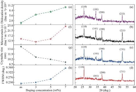
Fig. 1 X-Ray diffraction (a) as deposited SnO2, (b, c and d) 3wt%, 5wt% and 7wt%, respectively Co doping concentration, (e) Dislocation density, (f) Microstrain, (g) Crystallite size and (h) FWHM.
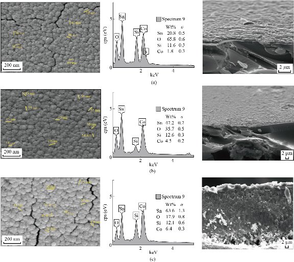
Fig. 2 SEM and EDXS of SnO2:Co (a) 3wt%, (b) 5wt% and (c) 7wt%.
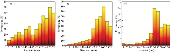
Fig. 3 Relation between diameter and percentage for SnO2:Co (a) 3wt%, (b) 5wt% and (c) 7wt%.
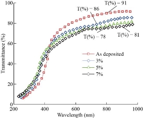
Fig. 4 Transmittance (%) versus wavelength for SnO2 and Co doped SnO2 films.
The optical energy gap
The direct energy gap was estimated for the relation (4), the direct band gap has been found to decline by increasing the doping percentage (3wt% and 5wt %) and increasing the band gap when doping increase at 7wt% due to the shift from Moss-Burstein [21-25].
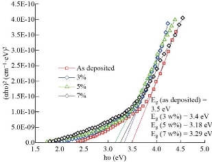
Fig. 5 (αhυ)2 versus photon energy for perspicuous and Cobalt transplantation SnO2.
Conclusions
In this paper, a methodology to obtain both pure and dopped SnO2 : Co thin films with tetragonal structure and similar chemical stoichiometry by RF magnetron sputtering using a target of pure tin is proposed. The maximum transmittance observed for un-doped SnO2 was almost (91%), while for the doped films was around 86% to 78%. The optical transmission values are decreasing with the increase cobalt concentration this behavior is may be due to the decreases in crystallite volume as measured using X-Ray diffraction and SEM observation the lower transmittance indicates higher defect density of the SnO2: Co films caused by crystalline defects such as grain boundaries and dislocations. This has resulted in decreasing the crystalline volume as demonstrated by structural measurements and SEM pictures, as well as the reduction of energy gap values due to the weakening of crystallization but not continuously the values of 7% increased the values of the energy gap by the effect of increasing the free shipping carriers in the energy gap.
Conflict of Interests
The authors declare that no competing interest exists.
Authors' Contribution
Ehssan Hassan contributed to 40% of the work, Mohamed Odda Dawod 30%, and Marwa Abdul Muhsien Hassan 30%.
Acknowledgments
This research was propped by University of Mustansiriyah, College of Science, Department of Physics, Tribology and advanced materials Lab. and the group labor would like to thank the Ministry of Science and technology for provided that the needful backing and advice for RF-magnetron sputtering setup. Financial grants in this paper were not achieved from any foundation.
References
Copyright© Ehssan Hassan, Mohamed Odda Dawod, Zainab Kadhom Hamzh, and Marwa Abdul Muhsien Hassan. This is an open-access article distributed under the terms of the Creative Commons Attribution License, which permits unrestricted use, distribution, and reproduction in any medium, provided the original author and source are credited.

|
Nano Biomedicine and Engineering. Copyright © Shanghai Jiao Tong University Press |
 |